Synchronous sram, Synchronous sram –38 – Altera Cyclone V E FPGA Development Board User Manual
Page 46
2–38
Chapter 2: Board Components
Memory
Cyclone V E FPGA Development Board
March 2013
Altera Corporation
Reference Manual
Synchronous SRAM
The development board supports a 18-Mb standard synchronous SRAM for
instruction and data storage with low-latency random access capability. The device
has a 1024K x 18-bits interface. This device is part of the shared FSM bus that connects
to the flash memory, SRAM, and MAX V CPLD 5M2210 System Controller.
The device speed is 250 MHz single-data-rate. There is no minimum speed for this
device. The theoretical bandwidth of this interface is 4 Gbps for continuous bursts.
The read latency for any address is two clocks while the write latency is one clock.
lists the SSRAM pin assignments, signal names, and functions.
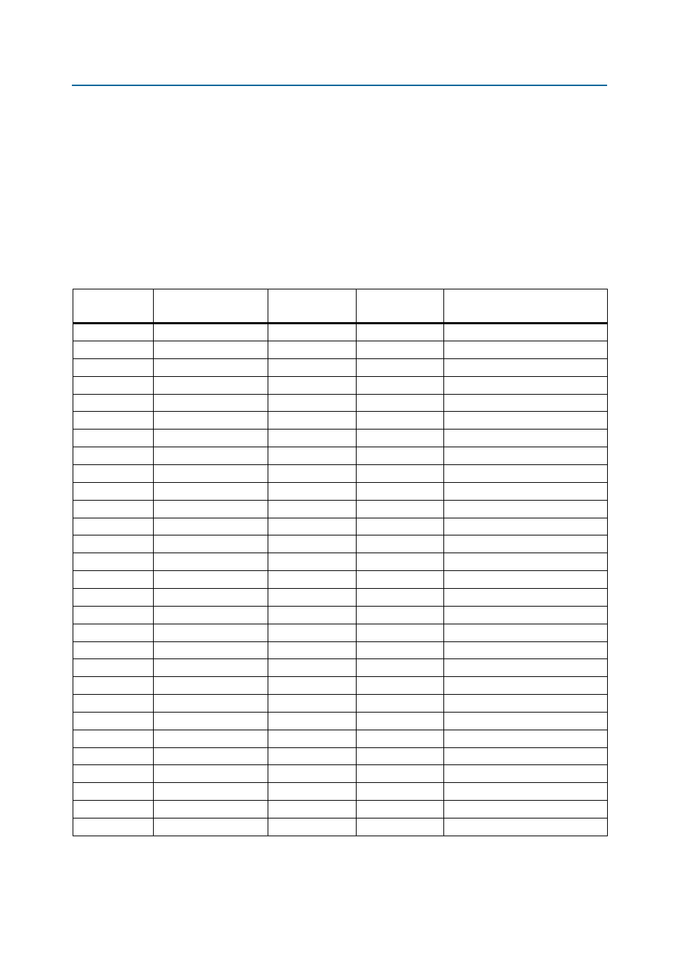
Table 2–27. SSRAM Pin Assignments, Schematic Signal Names, and Functions (Part 1 of 2)
Board
Reference (U11)
Schematic
Signal Name
Cyclone V E FPGA
Pin Number
I/O Standard
Description
86
SRAM_OEN
E7
2.5-V
Output enable
87
SRAM_WEN
D6
2.5-V
Write enable
37
FSM_A1
B11
2.5-V
Address bus
36
FSM_A2
A11
2.5-V
Address bus
44
FSM_A3
D9
2.5-V
Address bus
42
FSM_A4
C10
2.5-V
Address bus
34
FSM_A5
A10
2.5-V
Address bus
47
FSM_A6
A9
2.5-V
Address bus
43
FSM_A7
C9
2.5-V
Address bus
46
FSM_A8
B8
2.5-V
Address bus
45
FSM_A9
B7
2.5-V
Address bus
35
FSM_A10
A8
2.5-V
Address bus
32
FSM_A11
B6
2.5-V
Address bus
33
FSM_A12
A6
2.5-V
Address bus
50
FSM_A13
C7
2.5-V
Address bus
48
FSM_A14
C6
2.5-V
Address bus
100
FSM_A15
F13
2.5-V
Address bus
99
FSM_A16
E13
2.5-V
Address bus
82
FSM_A17
A5
2.5-V
Address bus
80
FSM_A18
A4
2.5-V
Address bus
49
FSM_A19
J7
2.5-V
Address bus
81
FSM_A20
H7
2.5-V
Address bus
39
FSM_A21
J9
2.5-V
Address bus
58
FSM_D0
F16
2.5-V
Data bus
59
FSM_D1
E16
2.5-V
Data bus
62
FSM_D2
M9
2.5-V
Data bus
63
FSM_D3
M8
2.5-V
Data bus
68
FSM_D4
F15
2.5-V
Data bus
69
FSM_D5
E15
2.5-V
Data bus