Eeprom, Eeprom –37 – Altera Cyclone V E FPGA Development Board User Manual
Page 45
Chapter 2: Board Components
2–37
Memory
March 2013
Altera Corporation
Cyclone V E FPGA Development Board
Reference Manual
EEPROM
This board includes a 64-Kb EEPROM device. This device has a 2-wire serial interface
bus I
2
C.
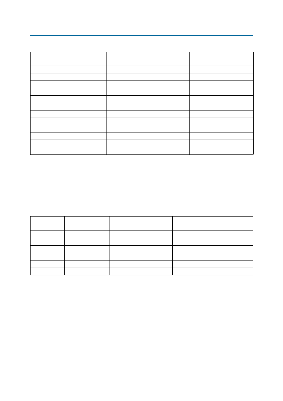
lists the EEPROM pin assignments, signal names, and functions. The signal
names and types are relative to the Cyclone V E FPGA in terms of I/O setting and
direction.
A14
LPDDR2_DQ29
—
1.2-V HSUL
Data bus byte lane 3
A13
LPDDR2_DQ30
—
1.2-V HSUL
Data bus byte lane 3
B12
LPDDR2_DQ31
—
1.2-V HSUL
Data bus byte lane 3
R23
LPDDR2_DQS0
V26
Differential 1.2-V HSUL
Data strobe P byte lane 0
P22
LPDDR2_DQSN0
U26
Differential 1.2-V HSUL
Data strobe N byte lane 0
J22
LPDDR2_DQS1
U27
Differential 1.2-V HSUL
Data strobe P byte lane 1
K23
LPDDR2_DQSN1
U28
Differential 1.2-V HSUL
Data strobe N byte lane 1
AB18
LPDDR2_DQS2
—
Differential 1.2-V HSUL
Data strobe P byte lane 2
AC19
LPDDR2_DQSN2
—
Differential 1.2-V HSUL
Data strobe N byte lane 2
B18
LPDDR2_DQS3
—
Differential 1.2-V HSUL
Data strobe P byte lane 3
A19
LPDDR2_DQSN4
—
Differential 1.2-V HSUL
Data strobe N byte lane 3
P1
LPDDR2_ZQ
—
1.2-V
ZQ impedance calibration
Table 2–25. LPDDR2 SDRAM Schematic Signal Names and Functions
Board
Reference (U9)
Schematic
Signal Name
Cyclone V E
FPGA Pin Number
I/O Standard
Description
Table 2–26. EEPROM Schematic Signal Names and Functions
Board
Reference (U12)
Schematic
Signal Name
Cyclone V E FPGA
Pin Number
I/O Standard
Description
1
EEPROM_A0
—
3.3-V
Chip address
2
EEPROM_A1
—
3.3-V
Chip address
3
EEPROM_A2
—
3.3-V
Chip address
5
EEPROM_SDA
AH7
3.3-V
Serial address or data
6
EEPROM_SCL
AG7
3.3-V
Serial clock
7
EEPROM_WP
—
3.3-V
Write protect input