Featured device: cyclone v e fpga, Featured device: cyclone v e fpga –4 – Altera Cyclone V E FPGA Development Board User Manual
Page 12
2–4
Chapter 2: Board Components
Featured Device: Cyclone V E FPGA
Cyclone V E FPGA Development Board
March 2013
Altera Corporation
Reference Manual
Featured Device: Cyclone V E FPGA
The Cyclone V E FPGA development board features a Cyclone V E FPGA
5CEFA7F31I7N device (U1) in a 896-pin FBGA package.
f
For more information about Cyclone V device family, refer to the
describes the features of the Cyclone V E FPGA 5CEFA7F31I7N device.
U10
Flash x16 memory
512-Mb synchronous flash devices with a 16-bit data bus for
non-volatile memory.
U11
SSRAM x16 memory
18-Mb standard synchronous RAM with a 12-bit data bus and 4-bit
parity.
U12
EEPROM
64-Mb I
2
C serial EEPROM.
Communication Ports
J1
HSMC port
Provides 84 CMOS or 17 LVDS channels per HSMC specification.
J11
Gigabit Ethernet port
RJ-45 connector which provides a 10/100/1000 Ethernet connection
via a Marvell 88E1111 PHY and the FPGA-based Altera Triple Speed
Ethernet MegaCore function in RGMII mode.
J12
Serial UART port
DSUB 9-pin connector with RS-232 transceiver to implement RS-232
serial UART channel.
J13
USB-UART port
USB connector with USB-to-UART bridge for serial UART interface.
J15, J16
Debug headers
Two 2×8 headers for debug purposes.
Video and Display Ports
J14 Character
LCD
Connector that interfaces to a provided 16 character × 2 line LCD
module along with two standoffs.
Power Supply
J17
DC input jack
Accepts a 14–20-V DC power supply.
SW5
Power switch
Switch to power on or off the board when power is supplied from the
DC input jack.
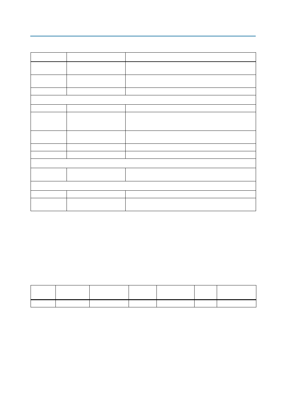
Table 2–1. Board Components (Part 3 of 3)
Board Reference
Type
Description
Table 2–2. Cyclone V E FPGA Features
ALMs
Equivalent LEs
M10K RAM Blocks
Total RAM
(Kbits)
18-bit × 18-bit
Multipliers
PLLs
Package Type
56,480
149,500
6,860
836
312
7
896-pin FBGA