Memory, Ddr3 sdram, Memory –32 – Altera Cyclone V E FPGA Development Board User Manual
Page 40: Ddr3 sdram –32
2–32
Chapter 2: Board Components
Memory
Cyclone V E FPGA Development Board
March 2013
Altera Corporation
Reference Manual
Memory
This section describes the development board’s memory interface support and also
their signal names, types, and connectivity relative to the Cyclone V E FPGA. The
development board has the following memory interfaces:
■
DDR3 SDRAM
■
LPDDR2 SDRAM
■
EEPROM
■
Synchronous SRAM
■
Synchronous flash
f
For more information about the memory interfaces, refer to the following documents:
■
section in the External Memory Interface Handbook.
■
section in the External Memory
Interface
DDR3 SDRAM
The development board supports two 16Mx16x8 and two 16Mx8x8 DDR3 SDRAM
interfaces for very high-speed sequential memory access.
The 32-bit data bus comprises of two x16 devices using soft memory controller (SMC)
interface. With SMC, this memory interface runs at a target frequency of 300 MHz for
a maximum theoretical bandwidth of over 9.6 Gbps. The maximum frequency for this
DDR3 device is 800 MHz with a CAS latency of 11.
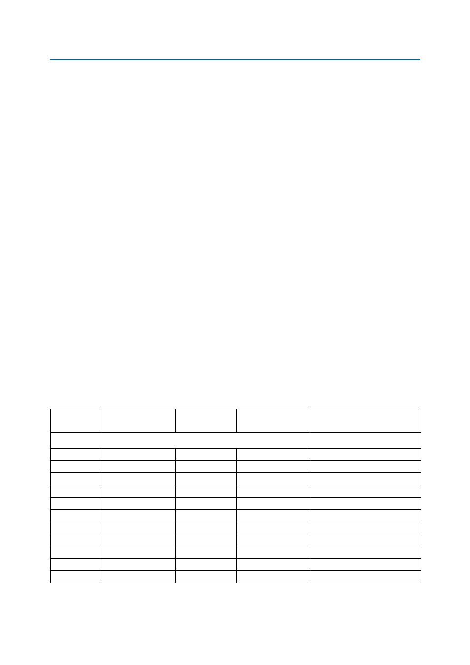
lists the DDR3 pin assignments, signal names, and functions. The signal
names and types are relative to the Cyclone V E FPGA in terms of I/O setting and
direction.
Table 2–24. DDR3 Device Pin Assignments, Schematic Signal Names, and Functions (Part 1 of 4)
Board
Reference
Schematic
Signal Name
Cyclone V E FPGA
Pin Number
I/O Standard
Description
DDR3 x16 (U8)
N3
DDR3_A0
A16
1.5-V SSTL Class I
Address bus
P7
DDR3_A1
G23
1.5-V SSTL Class I
Address bus
P3
DDR3_A2
E21
1.5-V SSTL Class I
Address bus
N2
DDR3_A3
E22
1.5-V SSTL Class I
Address bus
P8
DDR3_A4
A20
1.5-V SSTL Class I
Address bus
P2
DDR3_A5
A26
1.5-V SSTL Class I
Address bus
R8
DDR3_A6
A15
1.5-V SSTL Class I
Address bus
R2
DDR3_A7
B26
1.5-V SSTL Class I
Address bus
T8
DDR3_A8
H17
1.5-V SSTL Class I
Address bus
R3
DDR3_A9
D14
1.5-V SSTL Class I
Address bus
L7
DDR3_A10
E23
1.5-V SSTL Class I
Address bus