Altera Cyclone V E FPGA Development Board User Manual
Page 11
Chapter 2: Board Components
2–3
Board Overview
March 2013
Altera Corporation
Cyclone V E FPGA Development Board
Reference Manual
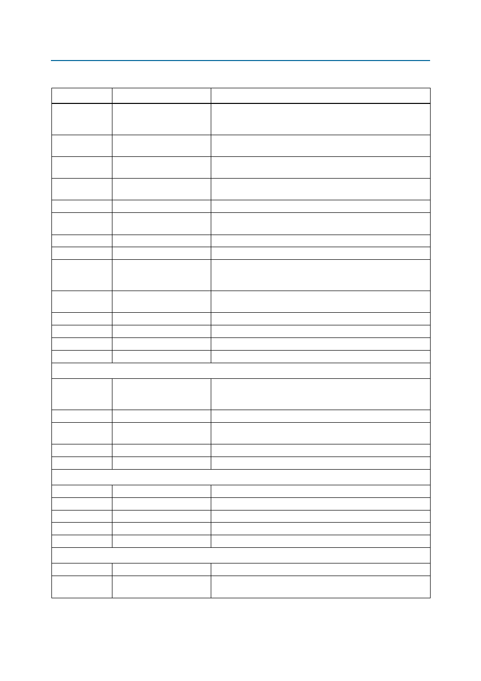
SW3
Board settings DIP switch
Controls the MAX V CPLD 5M2210 System Controller functions such
as clock enable, SMA clock input control, and which image to load
from flash memory at power-up.
SW1
MSEL DIP switch
Controls the configuration scheme on the board. MSEL pins 0, 1, 2 and
4 connects to the DIP switch while MSEL pin 3 connects to ground.
S2
Program select push button
Toggles the program select LEDs, which selects the program image
that loads from flash memory to the FPGA.
S1
Program configuration push
button
Load image from flash memory to the FGPA based on the settings of
the program select LEDs.
D19
Configuration done LED
Illuminates when the FPGA is configured.
D18
Load LED
Illuminates when the MAX V CPLD 5M2210 System Controller is
actively configuring the FPGA.
D17
Error LED
Illuminates when the FPGA configuration from flash memory fails.
D35
Power LED
Illuminates when 5.0-V power is present.
D25~D27
Program select LEDs
Illuminates to show the LED sequence that determines which flash
memory image loads to the FPGA when you press the program select
push button. Refer to
Table 2–6
for the LED settings.
D1~D10
Ethernet LEDs
Illuminates to show the connection speed as well as transmit or
receive activity.
D20, D21
HSMC port LEDs
You can configure these LEDs to indicate transmit or receive activity.
D22
HSMC port present LED
Illuminates when a daughter card is plugged into the HSMC port.
D15, D16
USB-UART LEDs
Illuminates when the USB-UART transmitter and receiver are in use.
D23, D24
Serial UART LEDs
Illuminates when UART transmitter and receiver are in use.
Clock Circuitry
X1
Programmable oscillator
Programmable oscillator with default frequencies of 125 MHz. The
frequency is programmable using the clock control GUI running on the
MAX V CPLD 5M2210 System Controller.
U4
50-MHz oscillator
50.000-MHz crystal oscillator for general purpose logic.
X3
100-MHz oscillator
100.000-MHz crystal oscillator for the MAX V CPLD 5M2210 System
Controller.
J2, J3
Clock input SMA connectors
Drive LVDS-compatible clock inputs into the clock multiplexer buffer.
J4
Clock output SMA connector
Drive out 2.5-V CMOS clock output from the FPGA.
General User Input/Output
D28~D31
User LEDs
Four user LEDs. Illuminates when driven low.
SW3
User DIP switch
Quad user DIP switches. When the switch is ON, a logic 0 is selected.
S4
CPU reset push button
Reset the FPGA logic.
S3
MAX V reset push button
Reset the MAX V CPLD 5M2210 System Controller.
S5~S8
General user push buttons
Four user push buttons. Driven low when pressed.
Memory Devices
U7, U8
DDR3 x32 memory
Two 256-MB DDR3 SDRAM with a 16-bit data bus.
U9
LPDDR2 x 16 memory
512-MB LPDDR 2 SDRAM with 32-bit bus, only 16-bit bus is used on
this board.
Table 2–1. Board Components (Part 2 of 3)
Board Reference
Type
Description