Debug header, Debug header –23 – Altera Cyclone V E FPGA Development Board User Manual
Page 31
Chapter 2: Board Components
2–23
General User Input/Output
March 2013
Altera Corporation
Cyclone V E FPGA Development Board
Reference Manual
lists the LCD pin definitions, and is an excerpt from Lumex data sheet.
f
For more information such as timing, character maps, interface guidelines, and other
related documentation, visi
Debug Header
This development board includes two 2×8 debug headers for debug purposes. The
FPGA I/Os route directly to the header for design testing, debugging, or quick
verification.
Table 2–19
summarizes the debug header pin assignments, signal names, and
functions.
4
LCD_D_Cn
AK11
2.5-V
LCD data or command select
5
LCD_WEn
AK10
2.5-V
LCD write enable
6
LCD_CSn
AJ12
2.5-V
LCD chip select
Table 2–17. Character LCD Pin Assignments, Schematic Signal Names, and Functions
Board
Reference (J14)
Schematic Signal Name
Cyclone V E FPGA
Pin Number
I/O Standard
Description
Table 2–18. LCD Pin Definitions and Functions
Pin
Number
Symbol
Level
Function
1
V
DD
—
Power supply
5 V
2
V
SS
—
GND (0 V)
3
V
0
—
For LCD drive
4
RS
H/L
Register select signal
H: Data input
L: Instruction input
5
R/W
H/L
H: Data read (module to MPU)
L: Data write (MPU to module)
6
E
H, H to L
Enable
7–14
DB0–DB7
H/L
Data bus—software selectable 4-bit or 8-bit mode
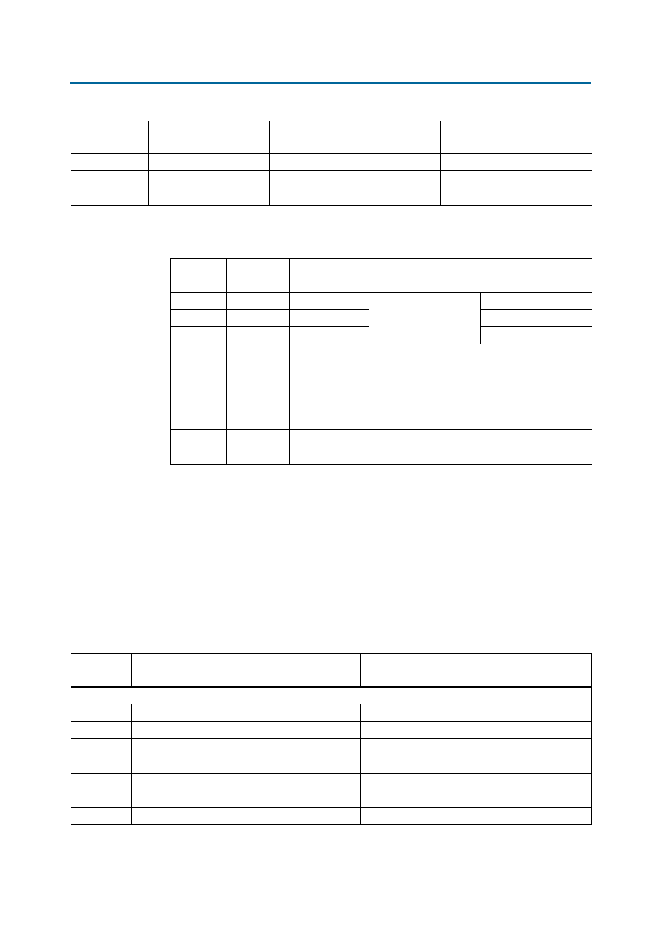
Table 2–19. Debug Header Pin Assignments, Schematic Signal Names, and Functions (Part 1 of 2)
Board
Reference
Schematic Signal
Name
Cyclone V E FPGA
Pin Number
I/O
Standard
Description
Debug Header (J15)
1
HEADER_D0
H21
1.5-V
Single-ended signal for debug purposes only
5
HEADER_D1
G21
1.5-V
Single-ended signal for debug purposes only
9
HEADER_D2
G22
1.5-V
Single-ended signal for debug purposes only
13
HEADER_D3
E26
1.5-V
Single-ended signal for debug purposes only
4
HEADER_D4
E25
1.5-V
Single-ended signal for debug purposes only
8
HEADER_D5
C27
1.5-V
Single-ended signal for debug purposes only
12
HEADER_D6
C26
1.5-V
Single-ended signal for debug purposes only