Altera Cyclone V E FPGA Development Board User Manual
Page 19
Chapter 2: Board Components
2–11
FPGA Configuration
March 2013
Altera Corporation
Cyclone V E FPGA Development Board
Reference Manual
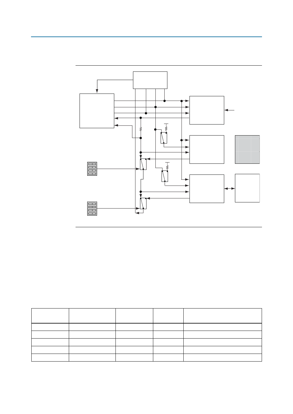
illustrates the JTAG chain.
The JTAG chain control DIP switch (SW2) controls the jumpers shown in
To connect a device or interface in the chain, their corresponding switch must be in
the OFF position. Slide all the switches to the ON position to only have the FPGA in
the chain.
1
The MAX V CPLD 5M2210 System Controller must be in the JTAG chain to use some
of the GUI interfaces.
lists the USB 2.0 PHY schematic signal names and their corresponding
Cyclone V E FPGA pin numbers.
Figure 2–3. JTAG Chain
Embedded
USB-Blaster II
GPIO
TCK
Cyclone V E
FPGA
Analog
Switch
MAX V CPLD
5M2210
System
Controller
HSMC
Port
GPIO
TMS
GPIO
TDO
GPIO
GPIO
TDI
JTAG Master
GPIO
Disable
Enable
Enable
JTAG Slave
HSMC
TCK
TMS
TDI
TDO
TCK
2.5 V
TMS
TDI
TDO
TCK
TMS
TDI
TDO
JTAG Slave
JTAG Slave
Analog
Switch
Always
Enabled
(in JTAG chain)
DIP Switch
DIP Switch
10-pin
JTAG Header
Flash
Memory
2.5 V
Table 2–5. USB 2.0 PHY Schematic Signal Names and Functions (Part 1 of 2)
Board Reference
(U18)
Schematic
Signal Name
Cyclone V E
FPGA Pin Number
I/O Standard
Description
C1
24M_XTALIN
—
3.3-V
Crystal oscillator input
C2
24M_XTALOUT
—
3.3-V
Crystal oscillator output
E1
FX2_D_N
—
3.3-V
USB 2.0 PHY data
E2
FX2_D_P
—
3.3-V
USB 2.0 PHY data
H7
FX2_FLAGA
—
3.3-V
Slave FIFO output status