Ftxl parallel i/o transceiver interface, The parallel communications interface – Echelon FTXL Hardware User Manual
Page 51

FTXL Hardware Guide
43
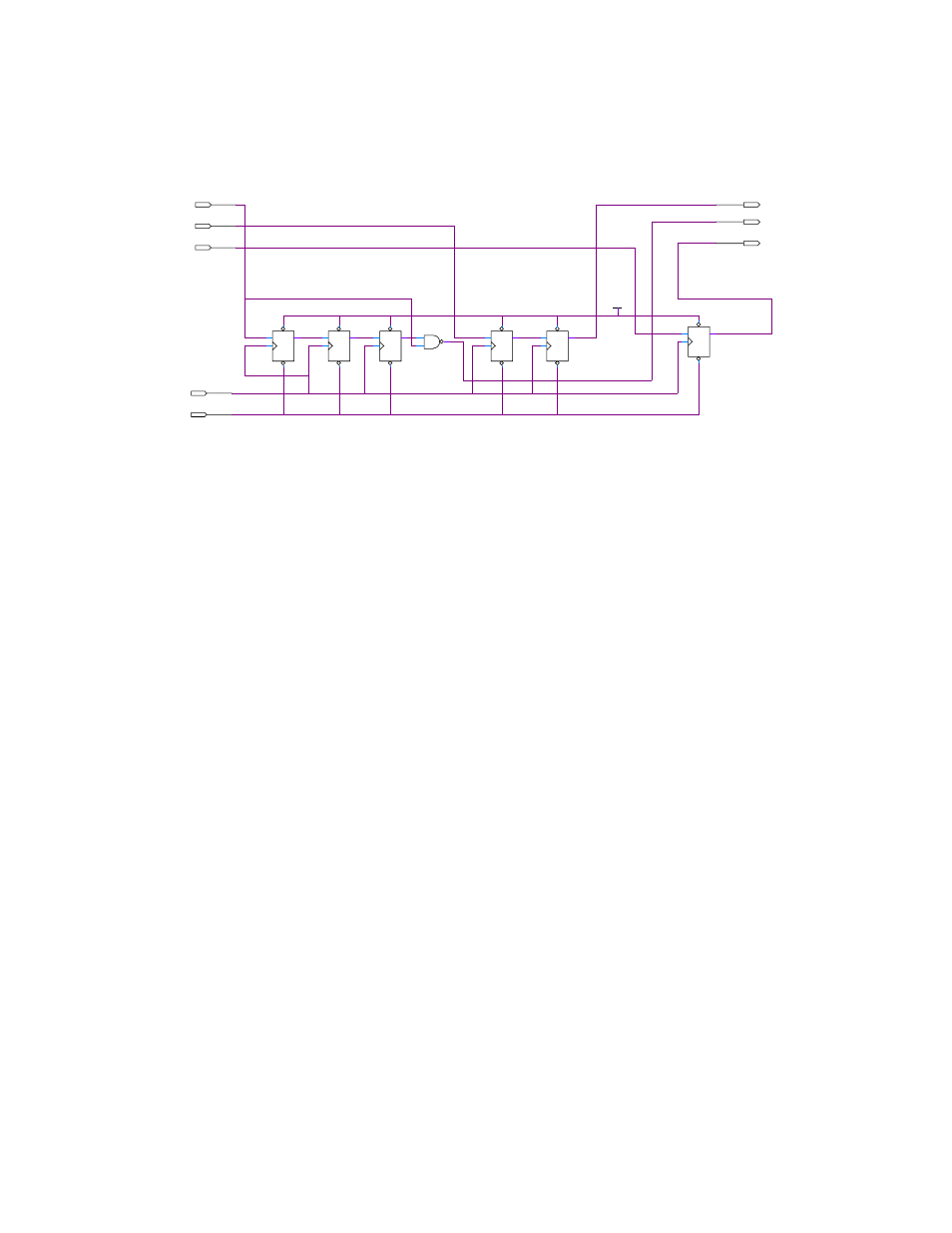
• The A0 signal is delayed by two clock cycles.
• The R/W~ signal is delayed by one clock cycle.
Figure 19 shows the circuit detail for this component.
VCC
CS_IN
INPUT
VCC
A0_IN
INPUT
VCC
RW_IN
INPUT
VCC
CLK_IN
INPUT
VCC
RESET_IN
INPUT
CS_OUT
OUTPUT
A0_OUT
OUTPUT
RW_OUT
OUTPUT
CLRN
D
PRN
Q
DFF
inst
CLRN
D
PRN
Q
DFF
inst2
CLRN
D
PRN
Q
DFF
inst5
CLRN
D
PRN
Q
DFF
inst6
NAND2
inst7
VCC
CLRN
D
PRN
Q
DFF
inst9
CLRN
D
PRN
Q
DFF
inst18
sy sclk
Figure 19. FTXL Parallel Interface Timing Delay Component
FTXL Parallel I/O Transceiver Interface
The FTXL parallel interface consists of a memory-mapped bus interface for an 8-
bit data bus and three 1-bit control signals, as described in
on page 21.
The FTXL parallel I/O transceiver interface component defines the following
signals, as shown in Figure 20 on page 44:
• clk_out: Component clock signal
• clk: Nios II processor clock signal
• address: FTXL address (A0) signal, that controls the function of the IO0
pin, which can be part of the data I/O (as D0) or can be the handshake
signal (as HS)
• data: FTXL data bus
• RW: FTXL read/write (R/W~) signal, which determines the direction of
the bidirectional data bus
• CS: FTXL chip select (CS~) signal, which specifies whether a byte-
transfer operation is in progress
Figure 20 on page 44 shows the definitions for the signals that comprise the
FTXL parallel interface. The figure shows part of the Quartus II Component
Editor dialog for this component, open to the Signals tab.
