Echelon FTXL Hardware User Manual
Page 30
22
FTXL Transceiver Hardware Interface
FTXL Transceiver
Pin Number
FTXL Transceiver
Pin Name
Signal Name
Direction
Note: Signal direction is from the point of view of the FTXL Transceiver Chip.
When configured in slave B mode, the Smart Transceiver defines a 3-bit control
port:
• IO8 is the chip select pin (CS~), and when asserted (driven low), specifies
that a byte-transfer operation is in progress. This pin is driven by the
FPGA device.
• IO9 is the read/write control pin (R/W~), and determines the direction of
the bidirectional data bus. When asserted (driven low), this pin indicates
a write operation; when deasserted (driven high), it specifies a read
operation. This pin is driven by the FPGA device.
• IO10 is the address pin (A0), and controls the function of the IO0 pin,
which can be part of the data I/O (as D0) or can be the handshake signal
(as HS). This pin is driven by the FPGA device.
The FTXL LonTalk protocol stack running on the Nios II processor in the FPGA
device manages the control port for the communications protocol with the FTXL
Transceiver.
Pins IO0-IO7 form the bidirectional data bus (D0-D7) when the IO10 (A0) pin is
low, or when the IO10 (A0) pin is high and the IO9 (R/W~) pin is low. The IO0
pin is the HS (handshake) acknowledgment signal to the master when the IO10
(A0) pin is high and IO9 (R/W~) is high. Table 11 summarizes the states of the
control port for determining the function of the IO0 (D0/HS) pin.
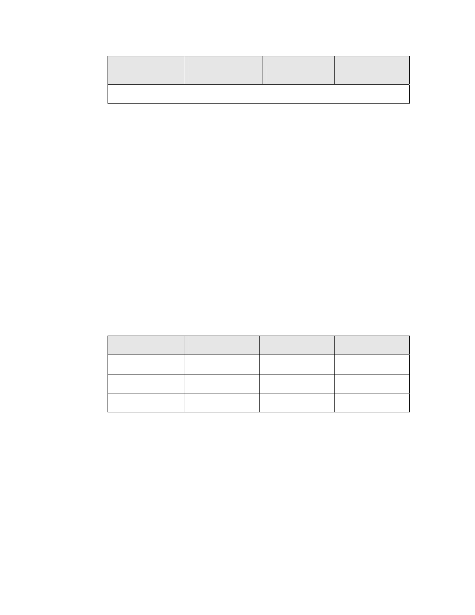
Table 11. Controlling the Function of the IO0 Pin
IO0 Function
CS~ State
A0 State
R/W~ State
D0 Low Low High
or
Low
D0 Low
High
Low
HS Low
High
High
The HS line is driven by the FTXL Transceiver. When it is high, it specifies that
the FTXL Transceiver is busy with an I/O operation, and cannot accept new
read/write requests. When it is low, the FPGA device can access the data bus. It
is possible for the state of the HS line to change before the CS~ pin becomes
inactive.