Fpga pin assignments for the ftxl transceiver – Echelon FTXL Hardware User Manual
Page 36
28
FTXL Transceiver Hardware Interface
When an externally generated clock is used to drive the CLK1 CMOS input pin of
the FTXL Transceiver, CLK2 must be left unconnected or used to drive no more
than one external CMOS load. The accuracy of the clock frequency must be
±0.02% (200 ppm) or better, to ensure that devices can correctly synchronize their
bit clocks.
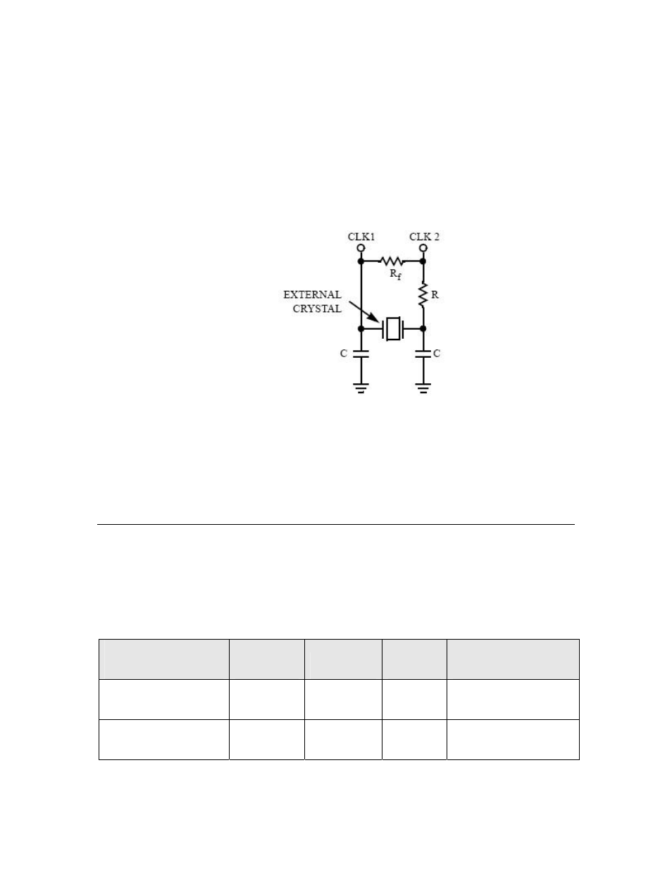
Figure 8 shows the crystal oscillator circuit. Use the load capacitance and
resistor values recommended by the manufacturer of the crystal for this circuit.
A 60/40 duty cycle or better is required when using an external oscillator. An
external oscillator must provide CMOS voltage levels to the CLK1 pin.
Figure 8. FTXL Transceiver Clock Generator Circuit
The FTXL Transceiver was designed to run at frequencies up to 40 MHz using an
external clock oscillator. External oscillators generally take several milliseconds
to stabilize after power-up. The FTXL Transceiver operating at 40 MHz must be
held in reset until the externally-generated CLK input is stable, so an external
power-on-reset-pulse stretching LVI chip/circuit is required. See the specification
for the oscillator for more information about startup stabilization times.
FPGA Pin Assignments for the FTXL Transceiver
The standard design that is included with the FTXL Developer’s Kit defines the
pins for communications with the FTXL Transceiver Chip, as listed in Table 12.
For your own FPGA design, you can assign the pins to any appropriate pins using
the Quartus II Pin Planner tool.
Table 12. FPGA Pin Assignments for the FTXL Transceiver
FPGA Design Pin
Name
FPGA Pin
Number
Direction
Edge
Capture
Corresponding FTXL
Transceiver Pin
FTXL_IRQ E20
Input
Rising
edge
Pin 24 (CP3/IRQ)
FTXL_SERVICE_PIN U1
Input
Either
edge
Pin 5 (SERVICE~)