Stacks, Data stack – Echelon Neuron User Manual
Page 32
...
lsb(ret)
msb(ret)
NEXT
...
GPR
0x0000
0xFFFF
BP
DSP
+
RSP
+
TOS
DSP -1
DSP -8
-1..-8
+
(DSP-relative
addressing mode)
256 Bytes
msb P0
lsb P0
msb P1
lsb P1
lsb P3
R0
R1
R15
BP +8
BP +0
BP +9
BP +23
General-Purpose
Registers
IP
Figure 2. Base Page Layout
Stacks
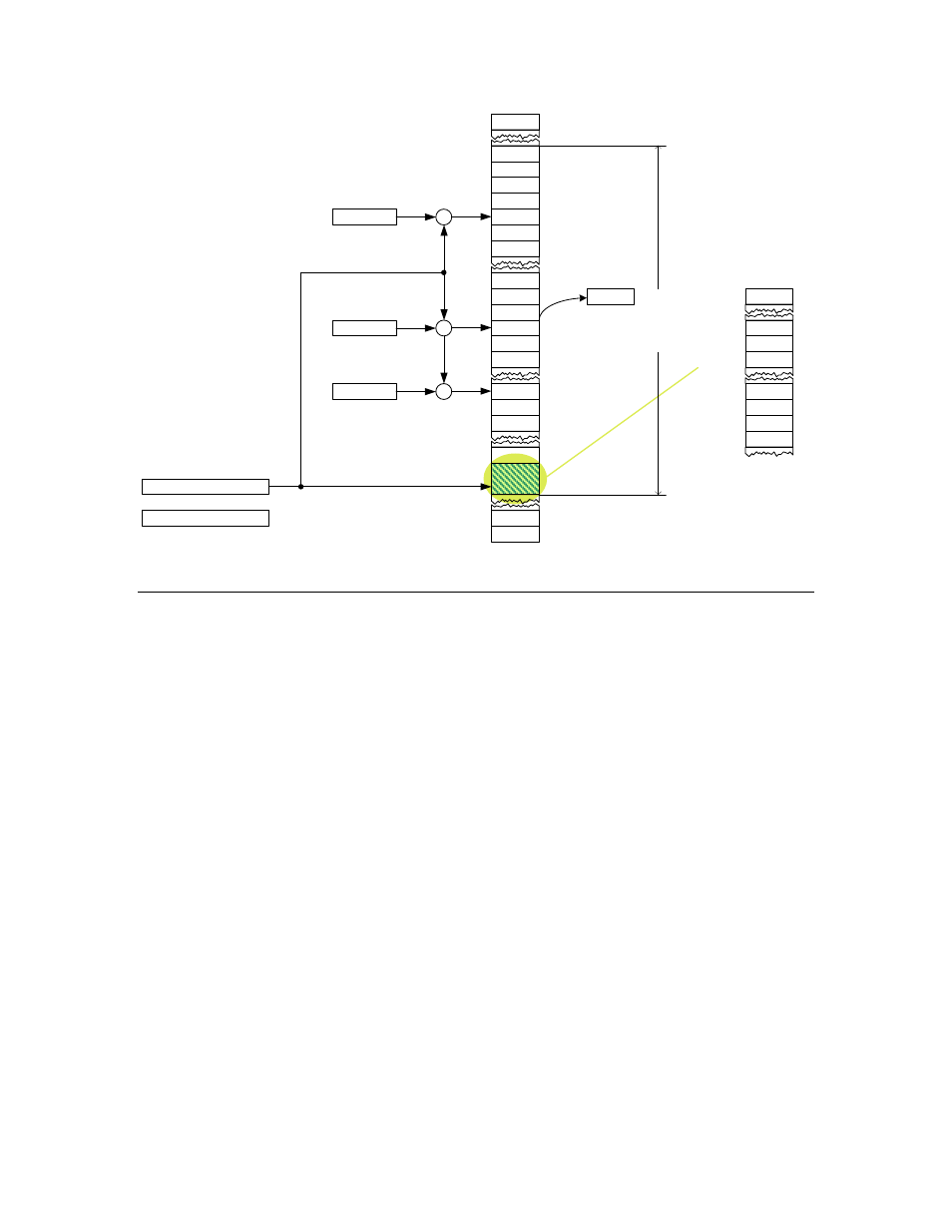
Each of the Neuron processors has two stacks: a data stack and a return stack.
The data stack starts at lower addresses and grows toward high memory. The
return stack starts at the top of the base page and grows toward low memory. In
general, it is up to the programmer to ensure that these two stacks do not
overlap.
Data Stack
The data stack is located both in registers and in base page RAM, that is, it
consists of two registers and associated memory. Access to the data stack is
controlled by two registers:
•
Top of stack (TOS) is an 8-bit data register that holds the top element of
the data stack.
•
Data stack register (DSP) is an 8-bit address register that, when added to
the BP, points to the location in the data stack where the NEXT element
exists. The DSP grows towards higher addresses.
Example: If the values 1, 2, 3, and 4 were on the data stack, and a PUSH
instruction pushed the value 5 onto the data stack, the register contents would be
as shown in Figure 3. Note that DSP points to the NEXT element.
22
Neuron Architecture for Neuron Assembly Programming