Solvline Eddy DK User Manual
Page 44
Eddy DK Programmer Guide
44
2.4.5.7. NAND Flash
- 256MB, 8bit Flash (Samsung K9F2G08U0A-PCB0)
- Chip Select #3 used, Address range : 0x4000_0000~0x4FFF_FFFF.
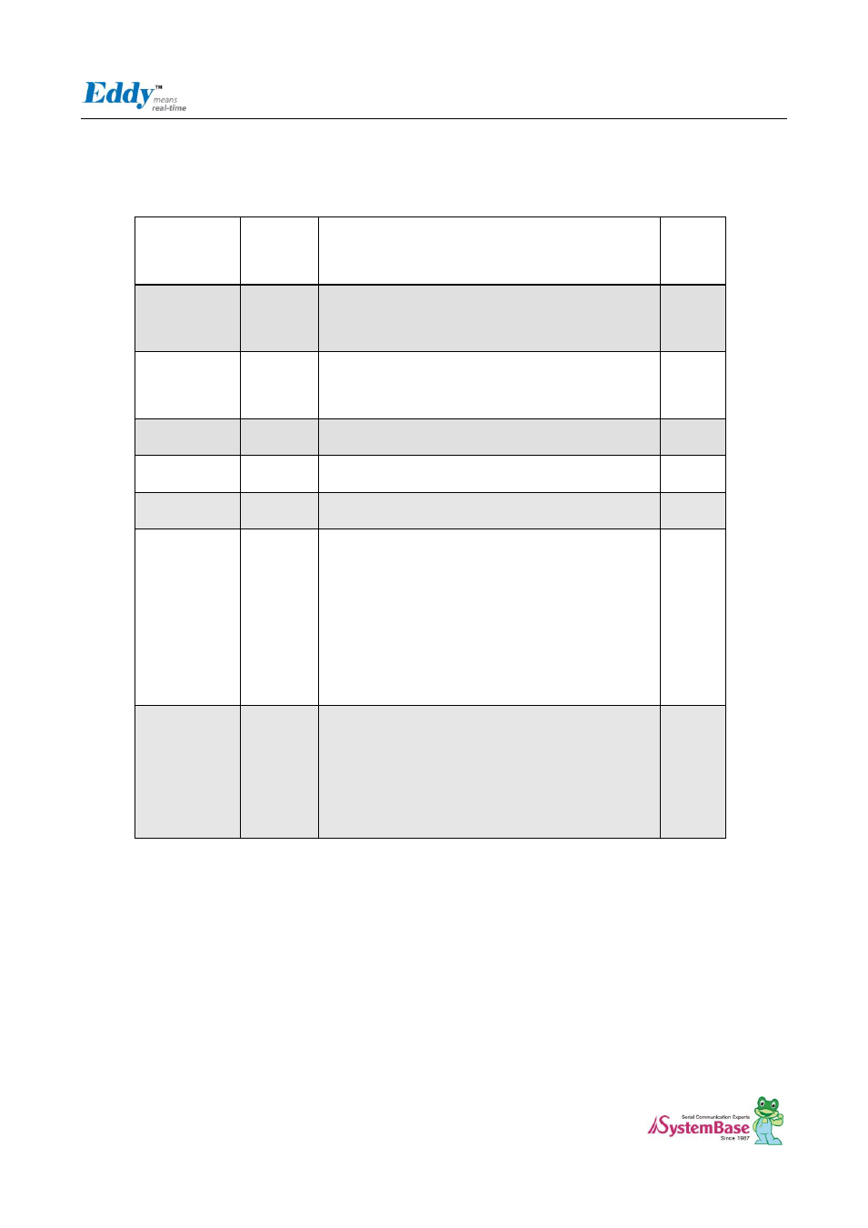
Eddy-CPU
v2.1 /v2.5
Signal Name
Function
Discription
I/O
A22
CLE
COMMAND LATCH ENABLE
The CLE input controls the activating path for
commands sent to the command register.
OUT
A21
ALE
ADDRESS LATCH ENABLE
The ALE input controls the activating path for
address to the internal address registers.
OUT
NANDOE
NANDOE data-out control
OUT
NANDWE
NANDWE controls writes to the I/O port
OUT
PC14(NCS3)
NANDCS device selection control
OUT
PC17
RDYBSY
(R/B)
READY/BUSY OUTPUT
The R/B output indicates the status of the device
operation. When low, it indicates that a program,
erase or random read operation is in process and
returns to high state upon completion. It is an
open drain output and
does not float to high-z condition when the chip
is deselected or when outputs are disabled.
IN
D[0:7]
DATA
bits
DATA INPUTS/OUTPUTS
The I/O pins are used to input command,
address and data, and to output data during read
operations. The I/O pins float to high-z when the
chip is deselected or when the outputs are
disabled.
I/O