J2 pin description – Solvline Eddy DK User Manual
Page 18
Eddy DK Programmer Guide
18
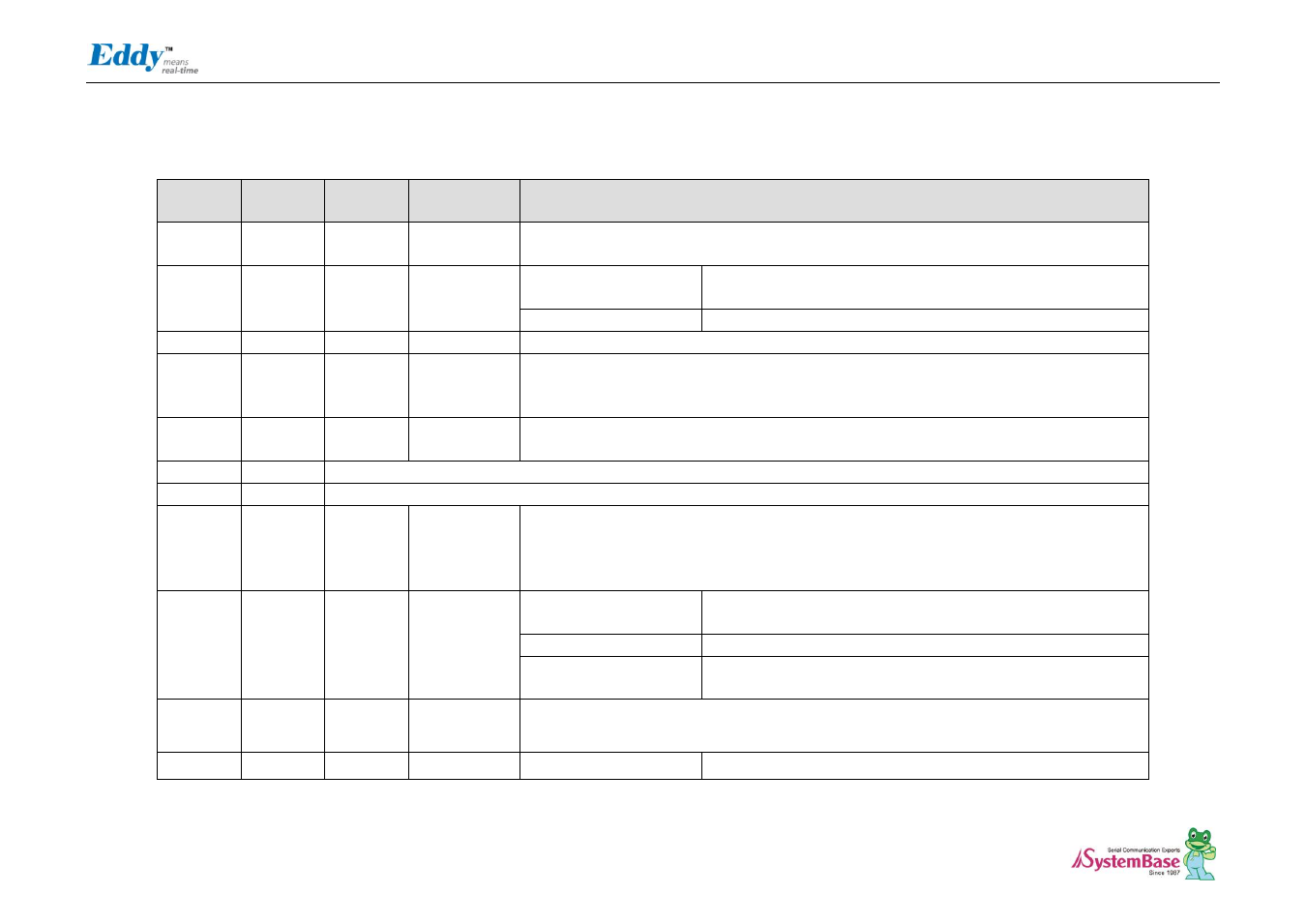
J2 Pin Description
Pin No
Name
DK v2.1
Pin No
Expansion
Header Pin No
Description
1~16
A[15:0]
J9_1
-J9_16
J3_4-J3_20
External Address Bus 0-15 (0 at reset)
DK is directly connected with CPU and external connecter (J3) is connected by buffer.
17
PC9
J9_17
J4_14
Peripheral A : NCS5
External device Chip Select 5.
256MB memory area addressable, active low
Peripheral B : TIOB0
Timer Counter ch0 I/O Line B
18
NEW
J9_18
J1_21
External device Write Enable signal, active low
19
FPG
J9_19
-
For Flash Programming
You can program Data Flash in Eddy CPU v2.1/v2.5 via USB. Refer to 2.4.2.3 S6:NAND Flash &
Data Flash Chip Select for further information.
20
NRD
J9_20
J1_23
External device Read Enable signal, active low
21, 23
GND
Ground
22, 24
3.3V
3.0V to 3.6V power input
25~32
D[7:0]
J9_25
- J3_32
J3_29 - J3_36
External Data Bus 0-7
DK is directly connected with CPU and external connecter (J3) is connected by buffer. You
should enable PC13(NCS6 : Chip Select 6) for working buffer, if you reset, it becomes Pulled-up
input.
33
PC13
J9_33
J4_18
Edd-DK v2.1 : NCS6
Data Bus connected with external header can be used when NCS6
is enabled.
Peripheral A : FIQ
Fast Interrupt Input
Peripheral B : NCS6
External device Chip Select 6
256MB memory area addressable, active low
34
JTAGSEL
J9_34
-
JTAG boundary scan can be used by connecting pin34 and 36(J14 connection). This pin should
not be connected when using ICE (In-Circuit Emulator) or in normal operation status.
35
PC12
J9_35
J4_17
Peripheral A : IRQ0
External Interrupt Input 0