J3 pin description – Solvline Eddy DK User Manual
Page 21
Eddy DK Programmer Guide
21
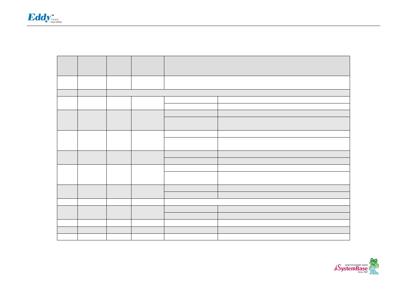
J3 Pin Description
Pin No
Name
DK v2.1
Pin No
Expansion
Header Pin
No
Description
1-5
PID[4:0]
J8_1
~J8_5
-
Product ID only used by the manufacturer.
Please do not work on these pins.
6,25,26
GND
Ground
7
PC14
J8_7
J4_19
Peripheral A : NCS3
External Device Chip Select 3
Peripheral B : IRQ2
External Interrupt Input 2
8
PC17
J8_8
J4_22
Peripheral A : D17
External Data Bus
Peripheral B :
SPI0_NPCS3
Disabled
9
PC18
J8_9
J4_23
Peripheral A : D18
External Data Bus
Peripheral B :
SPI1_NPCS1
SPI1(Serial Peripheral Interface) Peripheral Chip Select 1
10
PC8
J8_10
J4_13
Peripheral A : NCS4
External Device Chip Select 4
Peripheral B : RTS3
USART3 Request to Send
11
PC20
J8_11
J4_25
Peripheral A : D20
External Data Bus
Peripheral B :
SPI1_NPCS3
SPI1(Serial Peripheral Interface) Peripheral Chip Select 3
12
PC10
J8_12
J4_15
Peripheral A : A25
External Address Bus
Peripheral B : CTS3
USART3 Clear to Send
13
PA22
J8_13
-
Digital I/O Input 4
14
PC15
J8_14
J4_20
Peripheral A : NWAIT
External Wait Signal Input
Peripheral B : IRQ1
External Interrupt Input 2
15
PB8
J8_15
J2_9
Peripheral A : TXD2
UART2 Transmit Data
16
PB9
J8_16
J2_10
Peripheral A : RXD2
UART2 Receive Data
17
PB10
J8_17
J2_11
Peripheral A : TXD3
UART3 Transmit Data