Table 4-5: 71m6541 pin description table 3/3 – Maxim Integrated 71M6541 Demo Board User Manual
Page 74
71M6541 Demo Board REV 3.0 User’s Manual
74
Rev 4.0
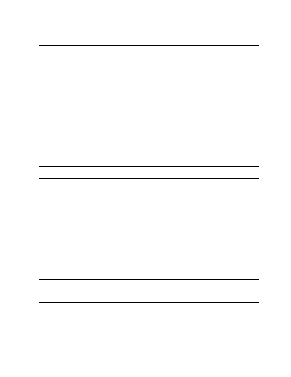
Digital Pins:
Table 4-4: 71M6541 Pin Description Table 3/3
Name
Type
Description
COM3,COM2,
COM1,COM0
O
LCD Common Outputs: These 4 pins provide the select signals for the
LCD display.
SEGDIO0 …
SEGDIO14,
SEGDIO19 …
SEGDIO25,
SEGDIO44,
SEGDIO45,
I/O
Multi-use pins, configurable as either LCD segment driver or DIO. Al-
ternative functions with proper selection of associated I/O RAM regis-
ters are:
SEGDIO0 = WPULSE
SEGDIO1 = VPULSE
SEGDIO2 = SDCK
SEGDIO3 = SDATA
SEGDIO6 = XPULSE
SEGDIO7 = YPULSE
Unused pins must be configured as outputs or terminated to
V3P3/GNDD.
SEGDIO26/ COM5,
SEGDIO27/ COM4
I/O
Multi-use pins, configurable as either LCD segment driver or DIO with
alternative function (LCD common drivers).
SEGDIO36/
SPI_CSZ,
SEGDIO37/ SPI_DO,
SEGDIO38/ SPI_DI,
SEGDIO39/ SPI_CKI
I/O
Multi-use pins, configurable as either LCD segment driver or DIO with
alternative function (SPI interface).
SEGDIO51/ OPT_TX,
SEGDIO55/ OPT_RX
I/O
Multi-use pins, configurable as either LCD segment driver or DIO with
alternative function (optical port/UART1)
E_RXTX/SEG48
I/O
Multi-use pins, configurable as either emulator port pins (when ICE_E
pulled high) or LCD segment drivers (when ICE_E tied to GND).
E_RST/SEG50
I/O
E_TCLK/SEG49
O
ICE_E
I
ICE enable. When zero, E_RST, E_TCLK, and E_RXTX become
SEG50, SEG49, and SEG48 respectively. For production units, this
pin should be pulled to GND to disable the emulator port.
TMUXOUT/ SEG47,
TMUX2OUT/ SEG46
O
Multi-use pins, configurable as either multiplexer/clock output or LCD
segment driver using the I/O RAM registers.
RESET
I
Chip reset: This input pin is used to reset the chip into a known state.
For normal operation, this pin is pulled low. To reset the chip, this pin
should be pulled high.
This pin has an internal 30 μA (nominal) current
source pulldown. No external reset circuitry is necessary.
RX
I
UART input. If this pin is unused it must be terminated to V3P3D
or GNDD.
TX
O
UART output.
TEST
I
Enables Production Test.
This pin must be grounded in normal operation.
PB
I
Push button input. This pin must be at GNDD when not active or unused.
A rising edge sets the IE_PB flag. It also causes the part to wake up if it is
in SLP or LCD mode. PB does not have an internal pullup or pulldown
resistor.
Pin types: P = Power, O = Output, I = Input, I/O = Input/Output,