4 71m6541 pinout information, 71m6541 pinout information, Table 4-3: 71m6541 pin description table 1/3 – Maxim Integrated 71M6541 Demo Board User Manual
Page 73: Table 4-4: 71m6541 pin description table 2/3
71M6541 Demo Board REV 3.0 User’s Manual
73
Rev 4.0
4.4 71M6541 PINOUT INFORMATION
Power/Ground/NC Pins:
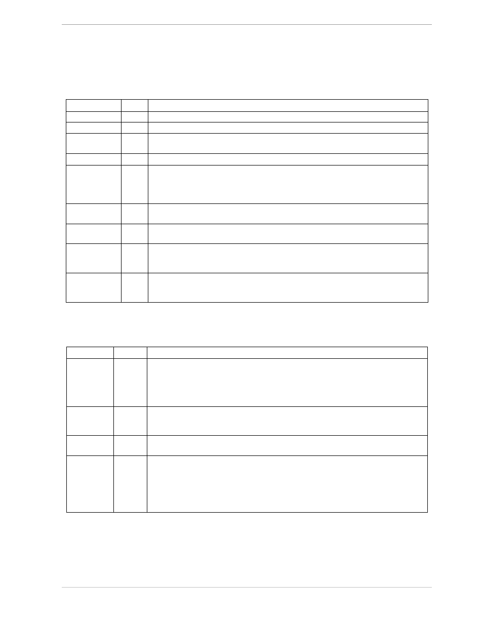
Table 4-2: 71M6541 Pin Description Table 1/3
Name
Type
Description
GNDA
P
Analog ground: This pin should be connected directly to the ground plane.
GNDD
P
Digital ground: This pin should be connected directly to the ground plane.
V3P3A
P
Analog power supply: A 3.3 V power supply should be connected to this pin.
V3P3A must be the same voltage as V3P3SYS.
V3P3SYS
P
System 3.3 V supply. This pin should be connected to a 3.3 V power supply.
V3P3D
O
Auxiliary voltage output of the chip. In mission mode, this pin is connected to
V3P3SYS by the internal selection switch. In BRN mode, it is internally con-
nected to VBAT. V3P3D is floating in LCD and sleep mode. A bypass capaci-
tor to ground should not exceed 0.1 µF.
VDD
O
The output of the 2.5V regulator. This pin is powered in MSN and BRN
modes. A 0.1 µF bypass capacitor to ground should be connected to this pin.
VLCD
O
The output of the LCD DAC. A 0.1 µF bypass capacitor to ground should be
connected to this pin.
VBAT
P
Battery backup pin to support the battery modes (BRN, LCD). A battery or
super-capacitor is to be connected between VBAT and GNDD. If no battery is
used, connect VBAT to V3P3SYS.
VBAT_RTC
P
RTC and oscillator power supply. A battery or super-capacitor is to be con-
nected between VBAT and GNDD. If no battery is used, connect VBAT_RTC
to V3P3SYS.
Analog Pins:
Table 4-3: 71M6541 Pin Description Table 2/3
Name
Type
Description
IAP/IAN,
IBP/IBN,
I
Differential or single-ended Line Current Sense Inputs: These pins are volt-
age inputs to the internal A/D converter. Typically, they are connected to the
outputs of current sensors. Unused pins must be tied to V3P3A.
Pins IBP/IBN may be configured for communication with the remote sensor
interface (71M6X0X).
VA
I
Line Voltage Sense Input: This pin is a voltage input to the internal A/D con-
verter. Typically, it is connected to the output of a resistor divider. Unused
pins must be tied to V3P3A.
VREF
O
Voltage Reference for the ADC. This pin should be left unconnected (float-
ing).
XIN
XOUT
I
O
Crystal Inputs: A 32 kHz crystal should be connected across these pins. Typi-
cally, a 15 pF capacitor is also connected from XIN to GNDA and a
10 pF capacitor is connected from XOUT to GNDA. It is important to minimize
the capacitance between these pins. See the crystal manufacturer datasheet
for details. If an external clock is used, a 150 mV (p-p) clock signal should be
applied to XIN, and XOUT should be left unconnected.
Pin types: P = Power, O = Output, I = Input, I/O = Input/Output