18 line length data register (11h), 19 output disable register (12h), 20 ais status register (13h) – Cirrus Logic CS61884 User Manual
Page 39: 21 ais interrupt enable register (14h), Line length data register (11h), See section, Line, Length data register (11h), See section 14.18 on
CS61884
DS485F3
39
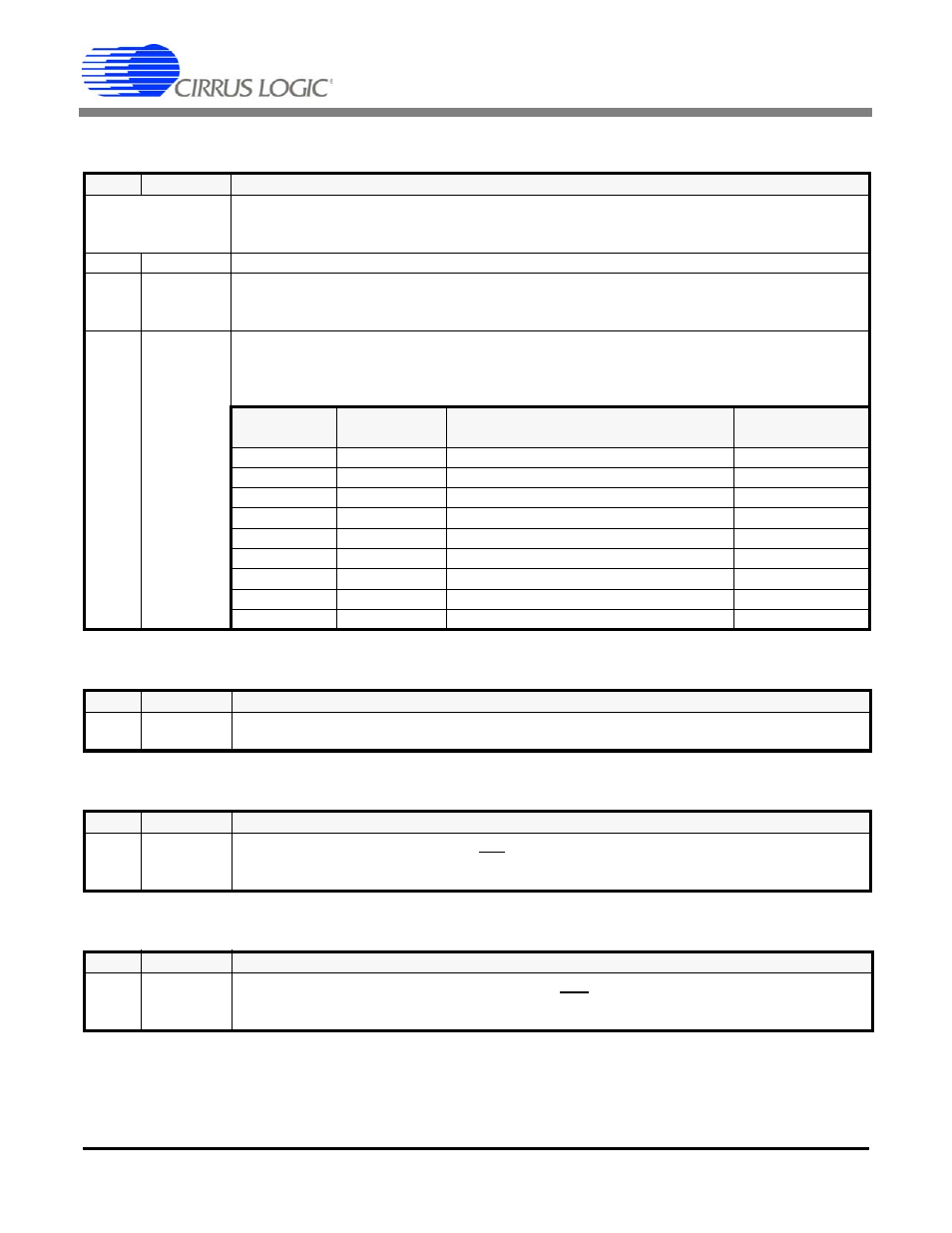
14.18 Line Length Data Register (11h)
14.19 Output Disable Register (12h)
14.20 AIS Status Register (13h)
14.21 AIS Interrupt Enable Register (14h)
BIT
NAME
Description
The value written to the 4-LSBs of this register specifies whether the device is operating in
either T1/J1 or E1 modes and the associated pulse shape as shown below is being transmit-
ted. Register bits default to 00h after power-up or reset.
[7:5]
RSVD
RESERVED (These bits must be set to 0.)
[4]
INT_EXTB
This bit specifies the use of internal (Int_ExtB = 1) or external (Int_ExtB = 0) receiver line
matching. The line impedance for both the receiver and transmitter are chosen through the
LEN [3:0] bits in this register.
[3:0]
LEN[3:0]
These bits setup the line impedance for both the receiver and the transmitter path and the
desired pulse shape for a specific channel. The channel is selected with the Line Length
Channel ID register (0x10). The following table shows the available transmitter pulse
shapes.
LEN [3:0]
Operation
Mode
Line Length Selection
Phase Samples
per UI
0000
E1
120
Ω 3.0V
12
0001
T1/J1
100
Ω DS1, Option A (undershoot)
14
0010
T1/J1
100
Ω DS1, Option A (0dB)
14
0011
T1/J1
100
Ω 0 - 133Ft (0.6dB)
13
0100
T1/J1
100
Ω 133 - 266Ft (1.2dB)
13
0101
T1/J1
100
Ω 266 - 399Ft (1.2dB)
13
0110
T1/J1
100
Ω 399 - 533Ft (2.4dB)
13
0111
T1/J1
100
Ω 533 - 655Ft (3.0dB)
13
1000
E1
75
Ω 2.37V
12
BIT
NAME
Description
[7:0]
OENB 7-0 Setting bit n of this register to “1” High-Z the TX output driver on channel n of the device.
Register bits default to 00h after power-up or reset.
BIT
NAME
Description
[7:0]
AISS 7-0
A “1” in bit position n indicates that the receiver has detected an AIS condition on channel n,
which generates an interrupt on the INT pin. Register bits default to 00h after power-up or
reset.
BIT
NAME
Description
[7:0]
AISE 7-0
This register enables changes in the AIS Status register to be reflected in the AIS Interrupt
Status register, thus causing an interrupt on the INT pin. Register bits default to 00h after
power-up or reset.