7 analog rx/tx data i/o – Cirrus Logic CS61884 User Manual
Page 19
CS61884
DS485F3
19
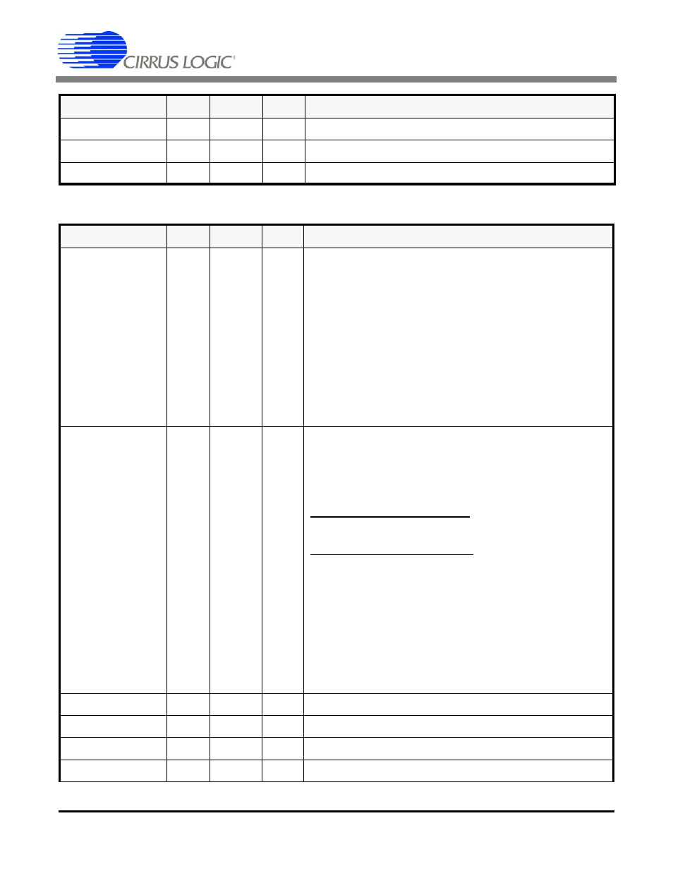
3.7 Analog RX/TX Data I/O
RCLK7
143
A1
O
Receive Clock Output Port 7
RPOS7/RDATA7
142
A2
O
Receive Positive Pulse/ Receive Data Output Port 7
RNEG7/BPV7
141
A3
O
Receive Negative Pulse/Bipolar Violation Output Port 7
SYMBOL
LQFP
LFBGA
TYPE
DESCRIPTION
SYMBOL
LQFP
LFBGA
TYPE
DESCRIPTION
TTIP0
TRING0
45
46
N5
P5
O
O
Transmit Tip Output Port 0
Transmit Ring Output Port 0
TTIP and TRING pins are the differential outputs of the
transmit driver. The driver internally matches impedances
for E1 75
Ω, E1 120 Ω and T1/J1 100 Ω lines requiring only
a 1:2 transformer. The CBLSEL pin is used to select the
appropriate line matching impedance only in “Hardware”
mode. In host mode, the appropriate line matching imped-
ance is selected by the
Line Length Data Register (11h)
(See Section 14.18 on page 39).
NOTE: TTIP and TRING are forced to a high impedance state
when the TCLK pin is “Low” for over 12
μS or the
TXOE pin is forced “Low”.
RTIP0
RRING0
48
49
P7
N7
I
I
Receive Tip Input Port 0
Receive Ring Input Port 0
RTIP and RRING are the differential line inputs to the re-
ceiver. The receiver uses either Internal Line Impedance or
External Line Impedance modes to match the line imped-
ances for E1 75
Ω, E1 120Ω or T1/J1 100Ω modes.
Internal Line Impedance Mode - The receiver uses the
same external resistors to match the line impedance (Refer
to
External Line Impedance Mode - The receiver uses differ-
ent external resistors to match the line impedance (Refer to
).
- In host mode, the appropriate line impedance is selected
by the
Line Length Data Register (11h)
14.18 on page 39).
- In hardware mode, the CBLSEL pin in combination with
the LEN pins select the appropriate line impedance. (Refer
to
for proper line impedance settings).
NOTE: Data and clock recovered from the signal input on
these pins are output via RCLK, RPOS, and RNEG.
TTIP1
52
L5
O
Transmit Tip Output Port 1
TRING1
51
M5
O
Transmit Ring Output Port 1
RTIP1
55
M7
I
Receive Tip Input Port 1
RRING1
54
L7
I
Receive Ring Input Port 1