4 register set, Table 9. host mode register set – Cirrus Logic CS61884 User Manual
Page 34
CS61884
34
DS485F3
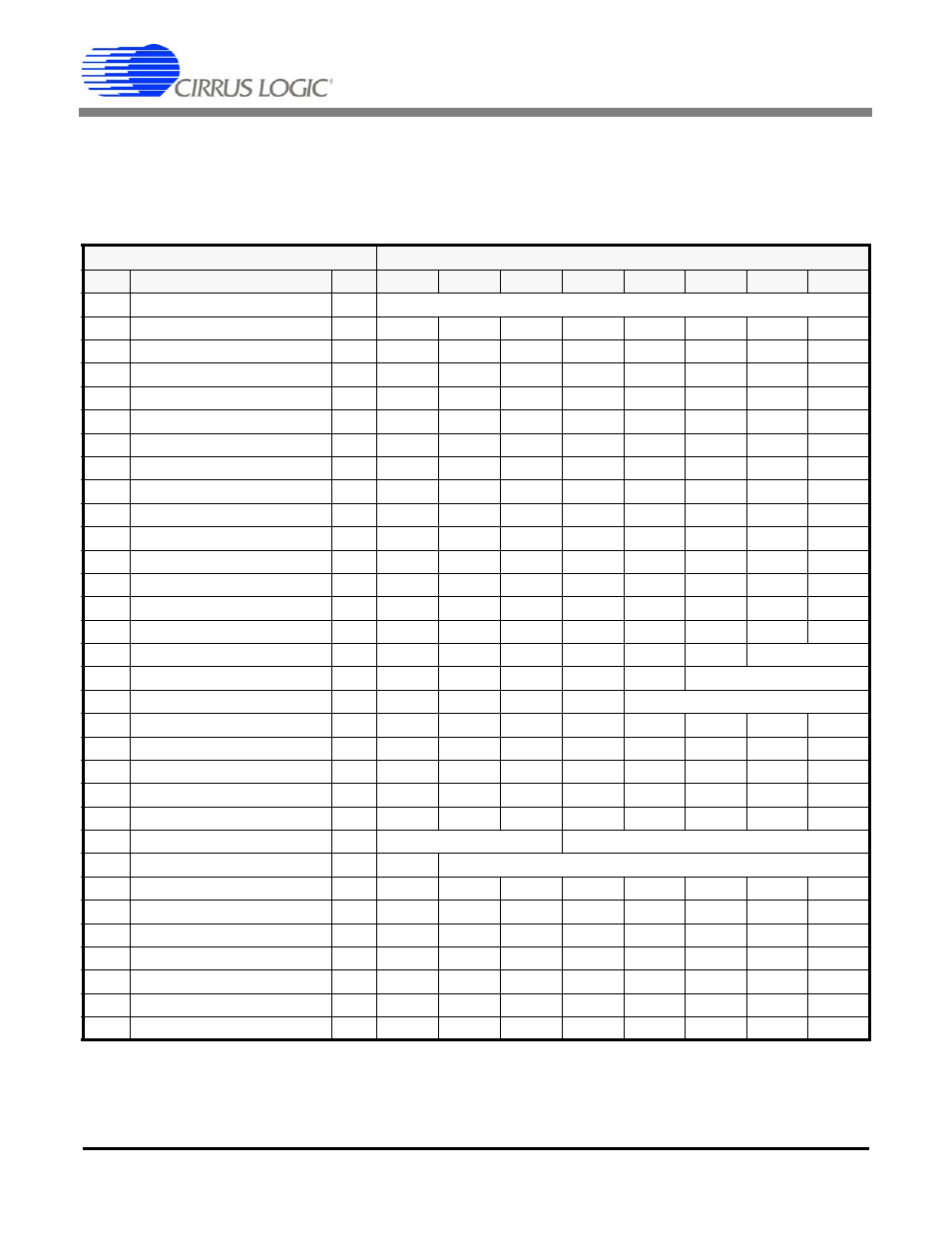
13.4 Register Set
The register set available during host mode opera-
tions are presented in
. While the upper
three bits of the parallel address are don’t cares on
the CS61884, they should be set to zero for proper
operation.
Table 9. Host Mode Register Set
REGISTERS
BITS
ADDR
NAME
TYPE
7
6
5
4
3
2
1
0
00h
Revision/IDCODE
R
IDCODE Refer to
01h
Analog Loopback
R/W
ALBK 7
ALBK 6
ALBK 5
ALBK 4
ALBK 3
ALBK 2
ALBK 1
ALBK 0
02h
Remote Loopback
R/W
RLBK 7
RLBK 6
RLBK 5
RLBK 4
RLBK 3 RLBK 2 RLBK 1
RLBK 0
03h
TAOS Enable
R/W
TAOE 7
TAOE 6
TAOE 5
TAOE 4 TAOE 3 TAOE 2 TAOE 1 TAOE 0
04h
LOS Status
R
LOSS 7 LOSS 6
LOSS 5
LOSS 4 LOSS 3 LOSS 2 LOSS 1 LOSS 0
05h
DFM Status
R
DFMS 7 DFMS 6 DFMS 5 DFMS 4 DFMS 3 DFMS 2 DFMS 1 DFMS 0
06h
LOS Interrupt Enable
R/W
LOSE 7 LOSE 6
LOSE 5
LOSE 4 LOSE 3 LOSE 2 LOSE 1 LOSE 0
07h
DFM Interrupt Enable
R/W
DFME 7 DFME 6 DFME 5 DFME 4 DFME 3 DFME 2 DFME 1 DFME 0
08h
LOS Interrupt Status
R
LOSI 7
LOSI 6
LOSI 5
LOSI 4
LOSI 3
LOSI 2
LOSI 1
LOSI 0
09h
DFM Interrupt Status
R
DFMI 7
DFMI 6
DFMI 5
DFMI 4
DFMI 3
DFMI 2
DFMI 1
DFMI 0
0Ah
Software Reset
R/W
SRES 7 SRES 6 SRES 5 SRES 4 SRES 3 SRES 2 SRES 1 SRES 0
0Bh
Performance Monitor
R/W
RSVD
RSVD
RSVD
RSVD
A3
A2
A1
A0
0Ch
Digital Loopback
R/W
DLBK 7
DLBK 6
DLBK 5
DLBK 4
DLBK 3 DLBK 2 DLBK 1
DLBK 0
0Dh
LOS/AIS Mode Enable
R/W
LAME 7 LAME 6 LAME 5 LAME 4 LAME 3 LAME 2 LAME 1 LAME 0
0Eh
Automatic TAOS
R/W
ATAO 7
ATAO 6
ATAO 5
ATAO 4
ATAO 3
ATAO 2
ATAO 1
ATAO 0
0Fh
Global Control
R/W
AI
Raisen
RSVD
Coden
FIFO
JACF
JASEL [1:0]
10h
Line Length Channel ID
R/W
RSVD
RSVD
RSVD
RSVD
RSVD
Channel ID
11h
Line Length Data
R/W
RSVD
RSVD
RSVD
IN_EX
LEN[3:0]
12h
Output Disable
R/W
OENB 7 OENB 6 OENB 5 OENB 4 OENB 3 OENB 2 OENB 1 OENB 0
13h
AIS Status
R
AISS 7
AISS 6
AISS 5
AISS 4
AISS 3
AISS 2
AISS 1
AISS 0
14h
AIS Interrupt Enable
R/W
AISE 7
AISE 6
AISE 5
AISE 4
AISE 3
AISE 2
AISE 1
AISE 0
15h
AIS Interrupt Status
R
AISI 7
AISI 6
AISI 5
AISI 4
AISI 3
AISI 2
AISI 1
AISI 0
16h
AWG Broadcast
R/W AWGB 7 AWGB 6 AWGB 5 AWGB 4 AWGB 3 AWGB 2 AWGB 1 AWGB 0
17h
AWG Phase Address
R/W
Channel Address [2:0]
Phase Address [4:0]
18h
AWG Phase Data
R/W
RSVD
Sample Data[6:0]
19h
AWG Enable
R/W AWGN 7 AWGN 6 AWGN 5 AWGN 4 AWGN 3 AWGN 2 AWGN 1 AWGN 0
1Ah
AWG Overflow Interrupt Enable R/W AWGE 7 AWGE 6 AWGE 5 AWGE 4 AWGE 3 AWGE 2 AWGE 1 AWGE 0
1Bh
AWG Overflow Interrupt Status
R
AWGI 7
AWGI 6
AWGI 5
AWGI 4
AWGI 3 AWGI 2 AWGI 1
AWGI 0
1Ch
RESERVED
R/W
RSVD 6 RSVD 5 RSVD 4 RSVD 3 RSVD 2 RSVD 1 RSVD 0 RSVD 6
1Dh
RESERVED
R
RSVD 6 RSVD 5 RSVD 4 RSVD 3 RSVD 2 RSVD 1 RSVD 0 RSVD 6
1Eh
BITS Clock Enable
R/W
BITS 7
BITS 6
BITS 5
BITS 4
BITS 3
BITS 2
BITS 1
BITS 0
1Fh
RESERVED
R/W
RSVD 7 RSVD 6 RSVD 5 RSVD 4 RSVD 3 RSVD 2 RSVD 1 RSVD 0