Cirrus Logic CS61884 User Manual
Features, Description

1
Copyright
Cirrus Logic, Inc. 2011
(All Rights Reserved)
CS61884
Octal T1/E1/J1 Line Interface Unit
Features
Industry-standard Footprint
Octal E1/T1/J1 Short-haul Line Interface Unit
Low Power
No external component changes for 100
Ω/120 Ω/75 Ω
operation.
Pulse shapes can be customized by the user.
Internal AMI, B8ZS, or HDB3 Encoding/Decoding
LOS Detection per T1.231, ITU G.775, ETSI 300-233
G.772 Non-Intrusive Monitoring
G.703 BITS Clock Recovery
Crystal-less Jitter Attenuation
Serial/Parallel Microprocessor Control Interfaces
Transmitter Short Circuit Current Limiter (<50mA)
TX Drivers with Fast High-Z and Power Down
JTAG boundary scan compliant to IEEE 1149.1.
144-Pin LQFP & 160-Pin LFBGA Packages
ORDERING INFORMATION
CS61884-IQZ
144-pin LQFP, Lead Free
CS61884-IRZ
160-pin LFBGA, Lead Free
Description
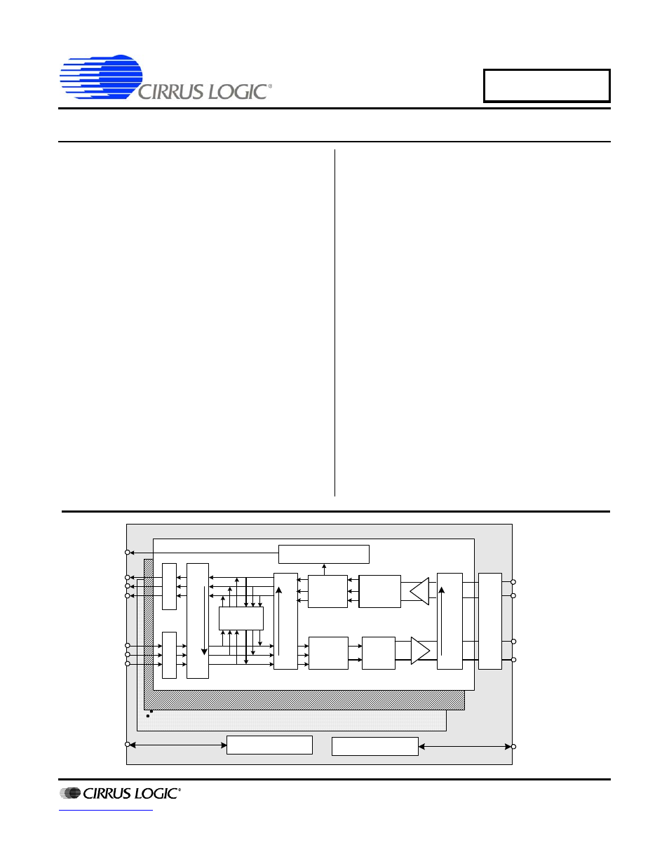
The CS61884 is a full-featured octal E1/T1/J1 short-haul
LIU that supports both 1.544 Mbps or 2.048 Mbps data
transmission. Each channel provides crystal-less jitter
attenuation that complies with the most stringent stan-
dards. Each channel also provides internal
AMI/B8ZS/HDB3 encoding/decoding. To support en-
hanced system diagnostics, channel zero can be
configured for G.772 non-intrusive monitoring of any of
the other 7 channels’ receive or transmit paths.
The CS61884 makes use of ultra-low-power, matched-
impedance transmitters and receivers to reduce power
beyond that achieved by traditional driver designs. By
achieving a more precise line match, this technique also
provides superior return loss characteristics. Additional-
ly, the internal line matching circuitry reduces the
external component count. All transmitters have controls
for independent power down and High-Z.
Each receiver provides reliable data recovery with over
12 dB of cable attenuation. The receiver also incorpo-
rates LOS detection compliant to the most recent
specifications.
RPOS
RNEG
TPOS
TNEG
TCLK
LOS
RTIP
RRING
TTIP
TRING
RCLK
0
1
7
JTAG Interface
Remot
e
Loopback
Digit
a
l Loopback
Analog Loopback
Decoder
Driver
Receiver
LOS
G.
772 Monit
o
r
Transmit
Control
Pulse
Shaper
Data
Recovery
Jitter
Attenuator
Clock
Recovery
Encoder
Host Interface
JTAG
Serial
Port
Host
Serial/Parallel
Port
MAR ‘11
DS485F3
Document Outline
- Features
- 1. Pinout - LQFP
- 2. Pinout - LFBGA
- 3. Pin Descriptions
- 4. Operation
- 5. Power-up
- 6. Master Clock
- 7. G.772 Monitoring
- 8. Building Integrated Timing Systems (Bits) Clock Mode
- 9. Transmitter
- 10. Receiver
- 11. Jitter Attenuator
- 12. Operational Summary
- 13. Host Mode
- 14. Register Descriptions
- 14.1 Revision/IDcode Register (00h)
- 14.2 Analog Loopback Register (01h)
- 14.3 Remote Loopback Register (02h)
- 14.4 TAOS Enable Register (03h)
- 14.5 LOS Status Register (04h)
- 14.6 DFM Status Register (05h)
- 14.7 LOS Interrupt Enable Register (06h)
- 14.8 DFM Interrupt Enable Register (07h)
- 14.9 LOS Interrupt Status Register (08h)
- 14.10 DFM Interrupt Status Register (09h)
- 14.11 Software Reset Register (0Ah)
- 14.12 Performance Monitor Register (0Bh)
- 14.13 Digital Loopback Reset Register (0Ch)
- 14.14 LOS/AIS Mode Enable Register (0Dh)
- 14.15 Automatic TAOS Register (0Eh)
- 14.16 Global Control Register (0Fh)
- 14.17 Line Length Channel ID Register (10h)
- 14.18 Line Length Data Register (11h)
- 14.19 Output Disable Register (12h)
- 14.20 AIS Status Register (13h)
- 14.21 AIS Interrupt Enable Register (14h)
- 14.22 AIS Interrupt Status Register (15h)
- 14.23 AWG Broadcast Register (16h)
- 14.24 AWG Phase Address Register (17h)
- 14.25 AWG Phase Data Register (18h)
- 14.26 AWG Enable Register (19h)
- 14.27 AWG Overflow Interrupt Enable Register (1Ah)
- 14.28 AWG Overflow Interrupt Status Register (1Bh)
- 14.29 Reserved Register (1Ch)
- 14.30 Reserved Register (1Dh)
- 14.31 Bits Clock Enable Register (1Eh)
- 14.32 Reserved Register (1Fh)
- 14.33 Status Registers
- 15. Arbitrary Waveform Generator
- 16. JTAG Support
- 17. Boundary Scan Register (BSR)
- 18. Applications
- 19. Characteristics and specifications
- 19.1 Absolute Maximum Ratings
- 19.2 Recommended Operating Conditions
- 19.3 Digital Characteristics
- 19.4 Transmitter Analog Characteristics
- 19.5 Receiver Analog Characteristics
- 19.6 Jitter Attenuator Characteristics
- 19.7 Master Clock Switching Characteristics
- 19.8 Transmit Switching Characteristics
- 19.9 Receive Switching Characteristics
- 19.10 Switching Characteristics - Serial Port
- 19.11 Switching Characteristics - Parallel Port (Multiplexed Mode)
- 19.12 Switching Characteristics- Parallel Port (Non-multiplexed Mode)
- 19.13 Switching Characteristics - JTAG
- 20. Compliant Recommendations and specifications
- 21. LFBGA package dimensions
- 22. LQFP Package dimensions
- 23. Ordering Information
- 24. Environmental, Manufacturing, & Handling Information
- 25. Revision History
