Transmitter – Cirrus Logic CS61884 User Manual
Page 24

CS61884
24
DS485F3
9. TRANSMITTER
The CS61884 contains eight identical transmitters
that each use a low power matched impedance driv-
er to eliminate the need for external load matching
resistors, while providing superior return loss. As a
result, the TTIP/TRING outputs can be connected
directly to the transformer allowing one hardware
circuit for 100
Ω (T1/J1), 120 Ω (E1), and 75 Ω
Digital transmit data is input into the CS61884
through the TPOS/TNEG input pins. These pins ac-
cept data in one of three formats: unipolar, bipolar,
or RZ. In either unipolar or bipolar mode, the
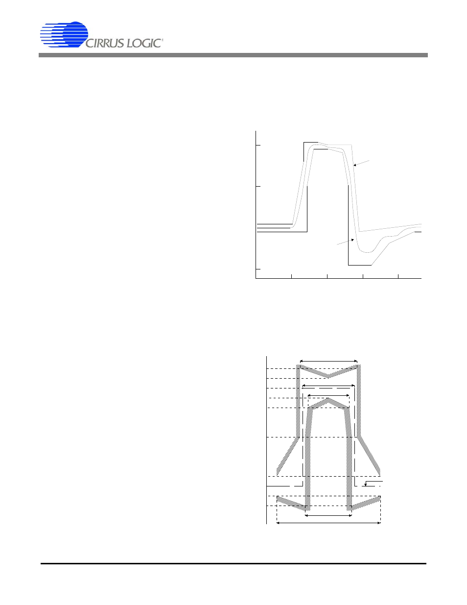
CS61884 internally generates a pulse shape com-
pliant to the ANSI T1.102 mask for T1/J1 or the
G.703 mask for E1 (Refer to
and
). The pulse shaping applied to the transmit
data can be selected in hardware mode or in host
mode.
In hardware mode, the pulse shape is selected for
all channels via the LEN[2:0] pins (Refer to
). This sets the pulse shape for
all eight transmitters to one of the prestored line
lengths. The CBLSEL pin in combination with the
LEN[2:0] pins set the line impedance for all eight
channels. The CBLSEL pin also selects between
E1 120
Ω or E1 75Ω modes, when the LEN pins are
configured for E1 operation mode.
In host mode, the pulse shape for each channel can
be set independently, during NRZ operation mode,
for proper clock recovery and jitter attenuation. In
RZ Mode each channel can be set to either T1/J1 or
E1, when there is no Mclk present (Refer to
To select the standard pulse shapes, the channels
are selected individually using the
page 38), then the LEN[3:0] bits in the
page 39) are set for the desired line length for that
channel. The LEN bits select the line type and im-
pedance for both the receiver and the transmitter of
the addressed channel.
NOTE: In host mode the CBLSEL pin is not used.
500
1.0
0.5
0
-0.5
0
250
750
1000
Normalized
Amplitude
Output Pulse
Shape
ANSI T1.102,
AT&T CB 119
Specifications
TIME (nanoseconds)
Figure 6. Pulse Mask at T1/J1 Interface
Figure 7. Pulse Mask at E1 Interface
269 ns
244 ns
194 ns
219 ns
488 ns
Nominal Pulse
0
10
50
80
90
100
110
120
-10
-20
Percent of
nominal peak
voltage
