Control and status, Control signals, Status signals – GE Industrial Solutions CAR2912TE series User Manual
Page 7: Car2912te series front-end, Preliminary data sheet
GE
Preliminary Data Sheet
CAR2912TE series front-end
Input: 90Vac to 264Vac; Output: 12Vdc @ 2900W; 3.3 or 5Vdc @ 4A Standby
October 21, 2013
©2013 General Electric Company. All rights reserved.
Page 7
Control and Status
Control hierarchy:
Some features, such as output voltage,
can be controlled both through hardware and firmware. For
example, the output voltage is controlled both by a signal pin
(Vprog) and a PMBus command, (OPERATION) .
Unless otherwise noted, the signal pin controls the feature
until the firmware command is executed. However, once the
firmware command has been executed, the signal pin is
ignored. In the above example, the power supply will no
longer ‘listen’ to the Vprog pin if the OPERATION command
has been executed.
In summary, Vprog is utilized for initialized configuration of
the output voltage and to change the output voltage when
PMBus is not used for that function.
Analog controls:
Details of analog controls are provided in
this data sheet under Feature Specifications.
Common ground:
All signals and outputs are referenced to
Output return.
Control Signals
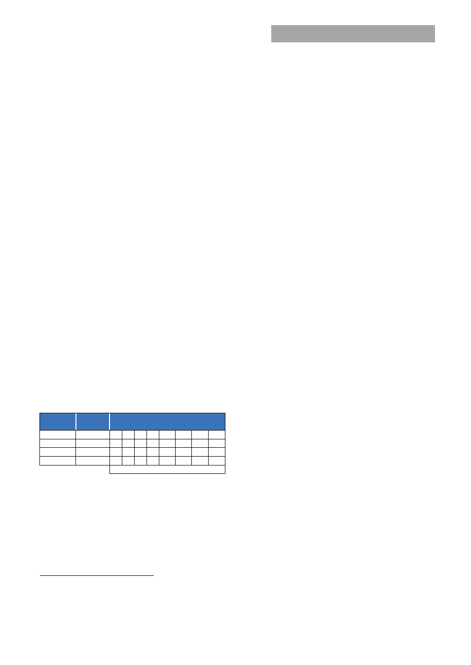
Device address:
Address bits A3, A2, A1, A0 configure the
specific address of the power supply. With these four bits, up
to sixteen (16) modules to be addressed on a single I²C bus.
The pins are pulled HI internal to the power supply. For a logic
LO these pins should be connected to ‘Output Return’. The
least significant bit x (LSB) of the address byte is set to either
write [0] or read [1]. A write command instructs the power
supply. A read command accesses information from the
power supply.
Device
Address
Address Bit Assignments
(Most to Least Significant)
7 6 5 4 3
2
1
0
MCU
C or Dx 1 1 0 A3 A2 A1 A0 R/W
Broadcast
00
0 0 0 0
0
0
0
0
ARA
12
0 0 0 1
1
0
0
1
MSB
LSB
Voltage programming (V
prog
):
An analog voltage on this
signal can vary the output voltage ± 10% from 10.8Vdc to
13.2Vdc.
Hardware voltage programming controls the output voltage
until a software margin command is executed. Software
voltage programming permanently overrides the hardware
margin setting and the power supply no longer listens to any
hardware margin settings until power to the controller is
7
Implement if feasible, this is a ‘read’ only address
interrupted, for example if input power or bias power is
recycled.
When bias power is recycled to the controller the controller
restarts into its default configuration, programmed to set the
output as instructed by the V
prog
pin. Again, subsequent
software commanded settings permanently override the
margin setting. As an example of an effective use of
hardware programming prior to the availability of software
based controls is to add a resistor between V
prog
and
Output_return. This is a way of changing the factory set point
of the front-end to whatever voltage level is desired by the
user during initial start-up.
Load share (I
share
):
This is a single wire analog signal that is
generated and acted upon automatically by power supplies
connected in parallel. I
share
pins should be connected to each
other for power supplies, if active current share among the
power supplies is desired. No resistors or capacitors should
get connected to this pin.
Remote ON/OFF:
Controls the presence of the main 12Vdc
output voltage. This is an open collector signal that needs to
be pulled HI externally through a resistor. A logic HI turns ON
the main output.
A turn OFF command either through this signal (ON/OFF) or
firmware commanded would turn OFF the 12V output.
Interlock:
This is a short signal pin that controls the presence
of the 12Vdc main output. This pin should be connected to
‘output return’ on the system side of the output connector.
The short pin ensures that no arcing or contact damage
occurs during the insertion/extraction process.
8V_INT:
Provides the ability to back_bias a front-end that lost
input power thus maintaining the ability to communicate with
a remote controller. This pin should be interconnected among
units in a system.
Status signals
See Feature Specifications for additional information
AC OK:
A TTL compatible status signal representing whether
the input voltage is within the anticipated range. This signal
needs to be pulled HI externally through a resistor.
DC OK:
A TTL compatible status signal representing whether
the output voltage is present. This signal needs to be pulled HI
externally through a resistor.
Over temp warning:
A TTL compatible status signal
representing whether an over temperature exists. This signal
needs to be pulled HI externally through a resistor.
If an over temperature should occur, this signal would pull LO
for approximately 10 seconds prior to shutting down the
power supply. In its default configuration, the unit would