C.11 d/a output channel 0 - base+10 and base+11, C.12 d/a output channel 1 - base+12 and base+13, C.13 d/a output channel 1 - base+12 and base+13 – B&B Electronics PCI-1711 - Manual User Manual
Page 95: Table c-13: register for d/a channel 0 data, Table c-14: register for load d/a channel 1 data, Table c-12, Register for load d/a channel 0 data, Table c-13, Register for d/a channel 0 data
Appendix C
– 87 –
PCI-1710 series User’s Manual
Advantech Co., Ltd.
www.advantech.com
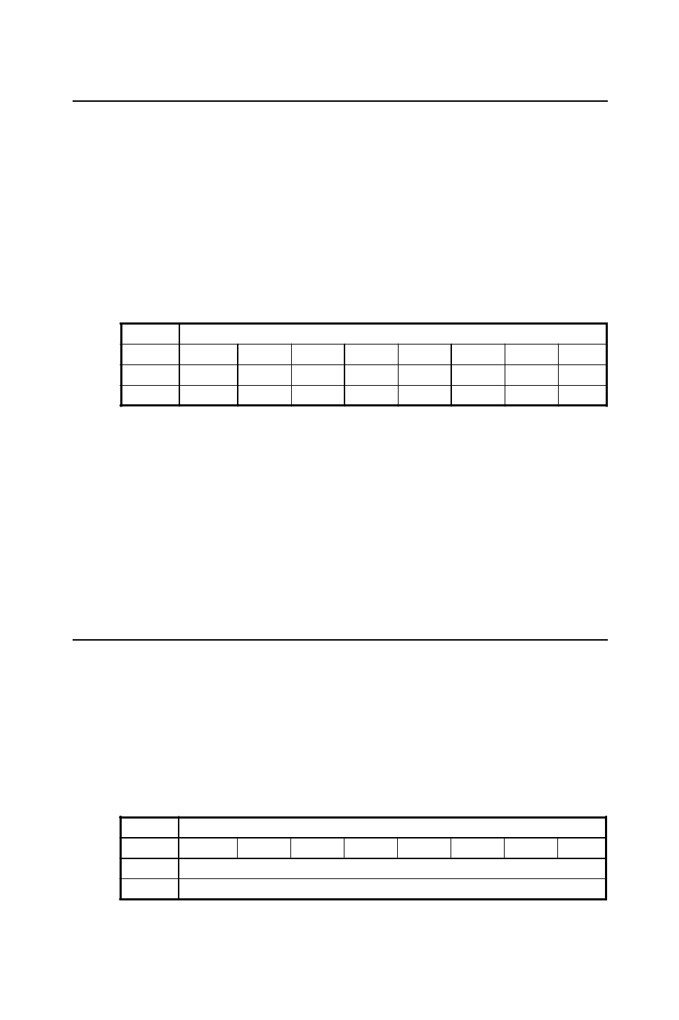
C.11 D/A Output Channel 0 - BASE+10 and BASE+11
The write-only registers of BASE+10 and BASE+11 accept data for D/
A Channel 0 output.
PCI-1710L/1710HGL/1711L/1716L
The PCI-1710L/1710HGL/1711L/1716L is not equipped with the D/A
functions.
PCI-1711/1710HG/1711/1716
Table C-13: Register for D/A channel 0 data
*: DA15, DA14, DA13, DA12 are only supported for PCI-1716/1716L
DA11 ~ DA0
Digital to analog data
DA0
LSB of the D/A data
DA11
MSB of the D/A data (for PCI-1710/1710L/1710HG/
1710HGL/1711/1711L)
DA15
MSB of the D/A data (for PCI-1716/1716L)
C.12 D/A Output Channel 1 - BASE+12 and BASE+13
The PCI-1716 provides the innovative design as gate control for
Analog Output function. It works as general Analog Output function
when you disable the flag (bit 11 (DA1_LDEN) of BASE+14). That
means the data will be output immediately. However, when you enable
the flag, you need to read these two registers BASE+12 and BASE+13
to output the data to the Analog Output channel.
Table C-14: Register for load D/A channel 1 data
Write
D/A Output Channel 0
Bit #
7
6
5
4
3
2
1
0
BASE + 11 *DA15
*DA14
*DA13
*DA12
DA11
DA10
DA9
DA8
BASE + 10
DA7
DA6
DA5
DA4
DA3
DA2
DA1
DA0
Read
Load D/A Channel 1 data
Bit #
7
6
5
4
3
2
1
0
BASE + 13
BASE + 12