Appendix a. specifications, Appendix b. block diagram, A. specifications – B&B Electronics PCI-1711 - Manual User Manual
Page 63: Appendix, Appendix a
Appendix A
– 55 –
PCI-1710 series User’s Manual
Advantech Co., Ltd.
www.advantech.com
Appendix
A
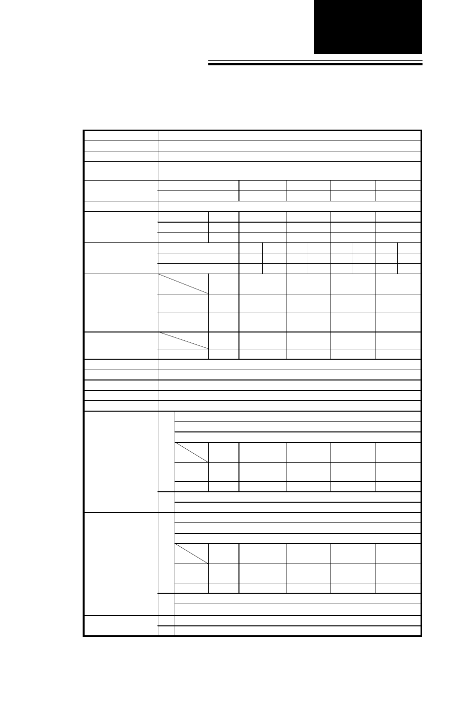
A. Specifications
PCI-1710/1710L/1710HG/1710HGL
Analog Input:
Channels
16 single-ended or 8 differential or combination
Resolution
12-bit
FIFO Size
4K samples
PCI-1710/1710L
Max. Sampling Rate1
100 KS/s
PCI-1710HG/1710HGL
Max. Sampling Rate
Gain
0.5, 1
5, 10
50, 100
500, 1000
Speed
100 KS/s
35 KS/s
7 KS/s
770 S/s
Conversion Time
8 µs
Input range and
Gain List for
PCI-1710/1710L
Gain
0.5
1
2
4
8
Unipolar
N/A
0~10
0~5
0~2.5
0~1.25
Bipolar
±10
±5
±2.5
±1.25
±0.625
Input range and Gain List
for PCI-
1710HG/1710HGL
Gain
0.5
1
5
10
50
100
500
1000
Unipolar
N/A
0~10
N/A
0~1
N/A
0~0.1
N/A 0~0.01
Bipolar
±10
±5
±1
±0.5
±0.1 ±0.05 ±0.01 ±0.005
Drift
1
2
4
8
16
Zero
(µV/º C)
15
15
15
15
15
Gain
(ppm//º C)
25
25
25
30
40
Small Signal Bandwidth
for PGA
1
2
4
8
16
Bandwidth
4.0 MHz
2.0 MHz
1.5 MHz
0.65 MHz
0.35 MHz
Common mode voltage
±11 V max. (operational)
Max. Input voltage
±15 V
Input Protect
30 Vp-p
Input Impedance
1 G
Ω
/5 pF
Trigger Mode
Software, on-board Programmable Pacer or External
PCI-1710/1710LAccuracy
DC
INLE: ±1 LSB
Monotonicity: 12 bits
Offset error: Adjustable to zero
0.5
1
2
4
8
Gain error
(% FSR)
0.01
0.01
0.02
0.02
0.04
Ch Type
S.E./D
S.E./D
S.E./D
D
D
AC
SNR: 68 dB
ENOB: 11 bits
PCI-1710HG/1710HGL
Accuracy
DC
INLE: ±1LSB
Monotonicity: 12 its
Offset error: Adjustable to zero
0.5,1
5,10
50,100
500
1000
Gain error
(% FSR)
0.01
0.02
0.04
0.08
0.08
Ch Type
S.E./D
S.E./D
D
D
D
AC
SNR: 68 dB
ENOB: 11 bits
External TTL Trigger
Input
Low
0.4 V max.
High
2.4 V min.
Gain
Gain
Gain
Gain