Chapter 5 – B&B Electronics PCI-1711 - Manual User Manual
Page 47
Chapter 5
– 39 –
PCI-1710 series User’s Manual
Advantech Co., Ltd.
www.advantech.com
A/D Calibration
Regular and accurate calibration procedures ensure the maximum
possible accuracy. The ADCAL.EXE calibration program leads you
through the whole A/D offset and gain adjustment procedure. The
basic steps are outlined below:
1. Set analog input channel AI0 as single-ended, bipolar, range ±5 V,
and set AI1 as single-ended, unipolar, range 0 to 10 V.
2. Connect a DC voltage source with value equal to 0.5 LSB (-4.9959
V) to AI0.
3. Adjust VR2 until the output codes from the card’s AI0 flickers
between 0 and 1.
4. Connect a DC voltage source with a value of 4094.5 LSB (4.9953 V)
to AI0.
5. Adjust VR3 until the output codes from the card’s AI0 flickers
between 4094 and 4095.
6. Repeat step 2 to step 5, adjusting VR2 and VR3.
7. Connect a DC voltage source with value equal to 0.5 LSB (1.22 mV)
to AI1.
8. Adjust VR1 until the output codes from the card’s AI1 flickers
between 0 and 1.
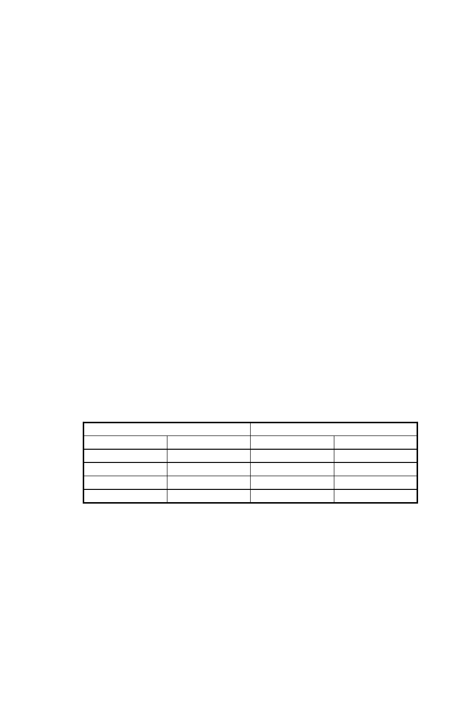
A/D code
Mapping Voltage
Hex.
Dec.
Bipolar ±5V
Unipolar 0 to 10V
000h
0
-4.9971 V
0 V
7FFh
2047
-0.0024 V
4.9947 V
800h
2048
0 V
4.9971 V
FFFh
4095
4.9947 V
9.9918 V
D/A Calibration (for PCI-1710/1710HG only)
In a way similar to the ADCAL.EXE program, the DACAL.EXE
program leads you through the whole D/A calibration procedure.
You can either use the on-board -5 V (-10 V) internal reference voltage
or use an external reference. If you use an external reference, connect a
reference voltage within the range ±10 V to the reference input of the
D/A output channel you want to calibrate. Adjust the full scale (gain)
of D/A channel 0 and 1, with VR4 and VR5 respectively.