E.2 d/a calibration (for pci-1716 only), Table e-1, A/d binary code table – B&B Electronics PCI-1711 - Manual User Manual
Page 110
Appendix E
– 102 –
PCI-1710 series User’s Manual
Advantech Co., Ltd.
www.advantech.com
6. Adjust UNIPOLAR offset voltage. First, writing any value to
BASE+9 to clear FIFO. Then to set A/D channel to channel 0, and
to set the range as 0 V to 10 V.
7. Writing the value from 0x0100 to 0x01FF sequentially to Calibra-
tion Command and Data register (BASE+18), and get each
bipolar range’s data by software trigger A/D method. Be noted that
to repeat this procedure 1000 times then to average those data for
each value. After that, to see whether the average data is close to
32767.5. If so, to go to next step. Otherwise, you must change the
value and repeat all the procedure in this step again until the
average data close to 32767.5.
8. Adjust GAIN offset voltage. First, writing any value to BASE+9 to
clear FIFO. Then to set A/D channel to channel 2, and to set the
range as -5 V to +5 V.
9. Writing the value from 0x0300 to 0x03FF sequentially to Calibra-
tion Command and Data register (BASE+18), and get each
bipolar range’s data by software trigger A/D method. Be noted that
to repeat this procedure 1000 times then to average those data for
each value. After that, to see whether the average data is close to
65534.6. If so, to go to next step. Otherwise, you must change the
value and repeat all the procedure in this step again until the
average data close to 65534.6.
10. Repeat steps 2 to 9 several times.
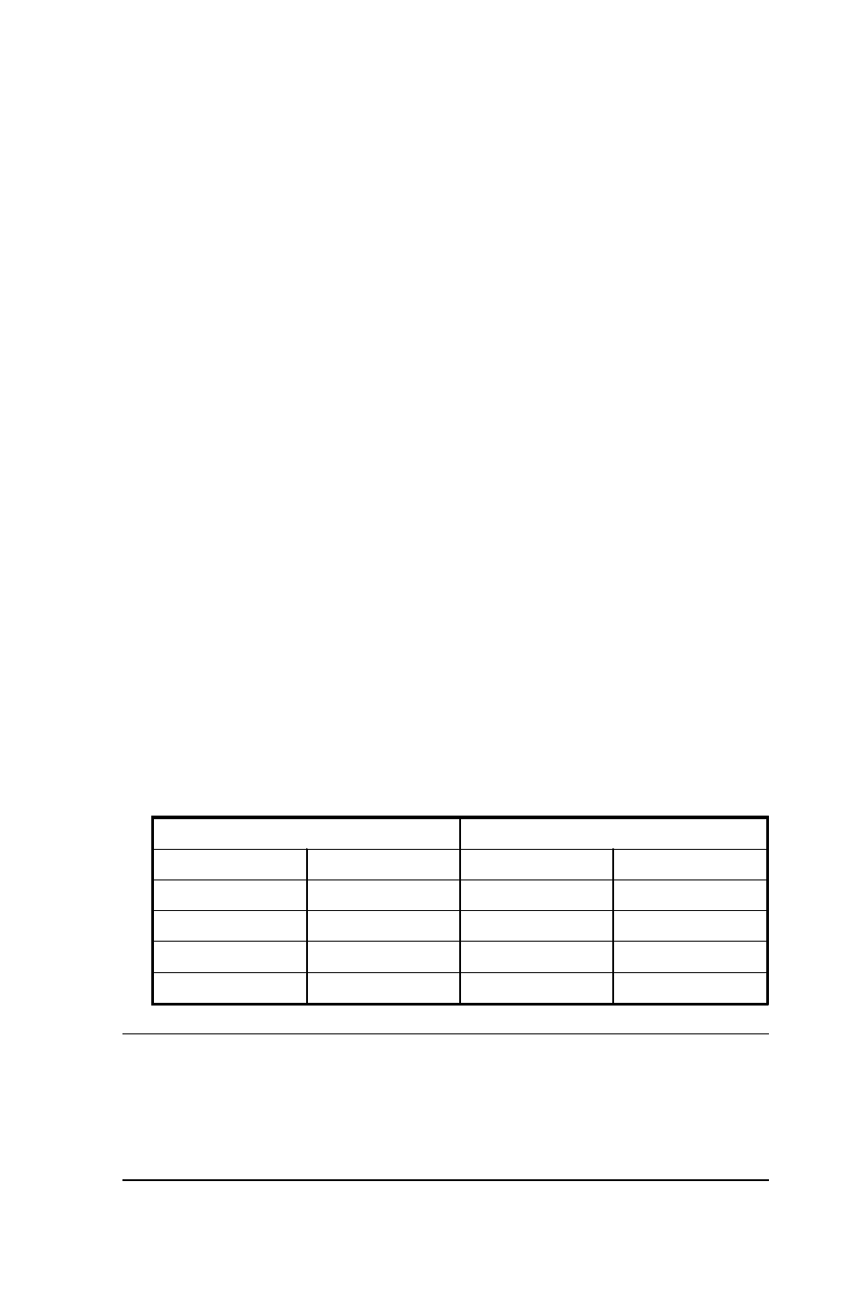
Table E-1: A/D binary code table
Note:
✎ 1 LSB = FS / 65535 for Unipolar (For example: 1LSB = 10 / 65535, while
the range is 0 V to10 V)
✎ 1 LSB = +FS / 32768 for Bipolar (For example: 1LSB = 5 / 32768, while
the range is -5 V to +5 V)
A/D code
Mapping Voltage
Hex.
Dec.
Bipolar
Unipolar
0000h
0
-FS
0
7FFFh
32767
-1 LSB
0.5 FS - 1 LSB
8000h
32768
0
0.5 FS
FFFFh
65535
+FS - 1 LSB
FS - 1 LSB