Combination mode timer 3 and ssi, Combination mode 6: fsk modulation, Atar862-8 – Rainbow Electronics ATAR862-8 User Manual
Page 81: Figure 81, Combination timer 3 and ssi

81
ATAR862-8
4589B–4BMCU–02/03
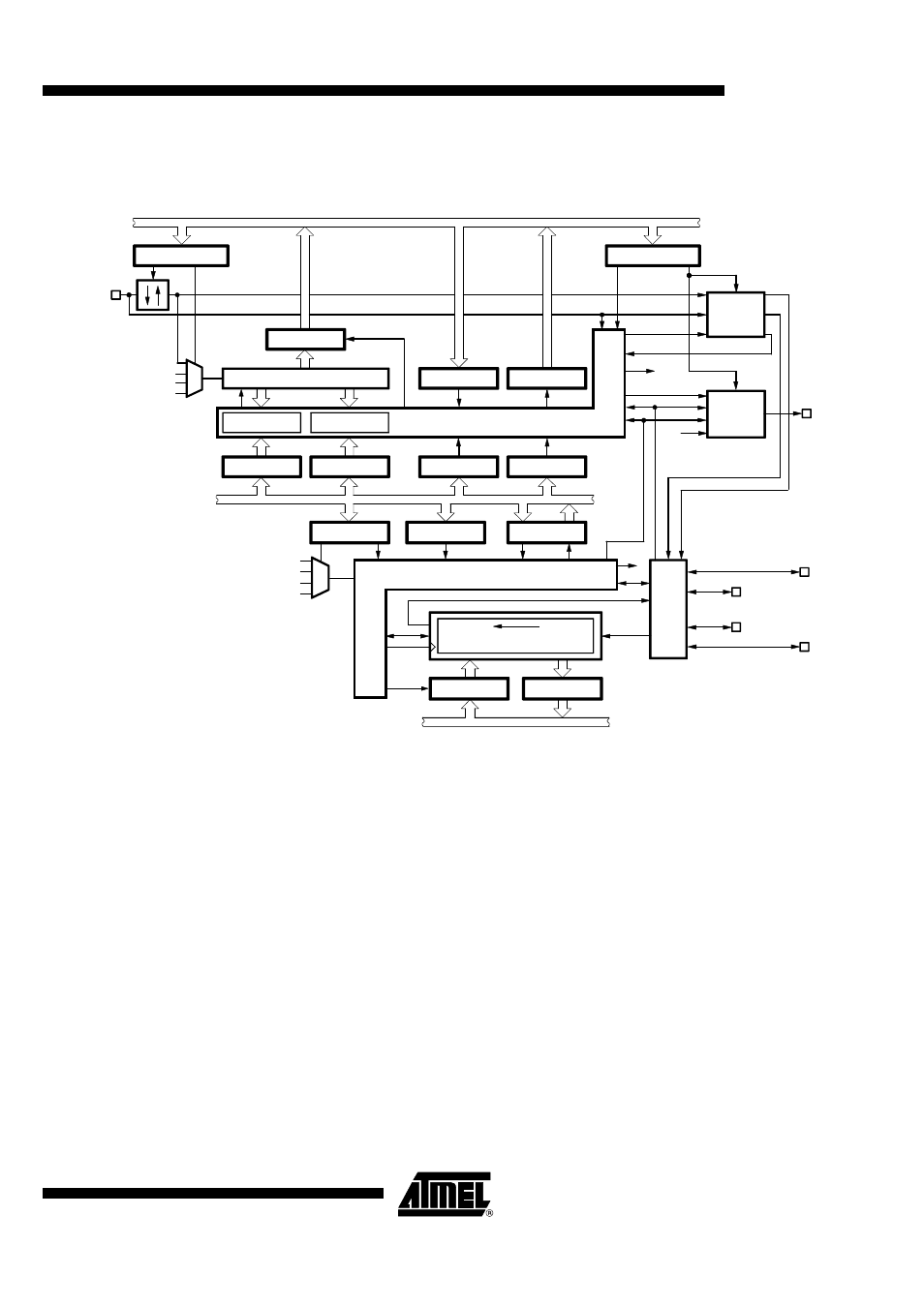
Combination Mode Timer 3 and SSI
Figure 81.
Combination Timer 3 and SSI
Combination Mode 6:
FSK Modulation
SSI mode 1:
8-bit shift register internal data output (SO) to the Timer 3
Timer 3 mode 8: FSK modulation with shift register data (SO)
The two compare registers are used to generate two varied time intervals. The SSI data
output selects which compare register is used for the output frequency generation. A "0"
level at the SSI data output enables the compare register 1 and a "1" level enables the
compare register 2. The compare and compare mode registers must be programmed to
generate the two frequencies via the output toggle flip-lop. The SSI can be supplied with
the toggle signal of Timer 2 or any other clock source. The Timer 3 counter is driven by
an internal or external clock source.
8-bit counter 3
RES
Compare 3/1
T3CO1
T3CP
T3CO2
Timer 3 - control
T3O
CL3
T3I
T3EX
SYSCL
T1OUT
POUT
I/O-bus
Compare 3/2
T3CM1
T3CM2
T3C
T3ST
Modulator 3
Demodu-
lator 3
M2
Control
SO
TOG3
INT5
RES
CM31
T3I
T3EX
SI
SC
T3M
T3CS
CP3
8-bit shift register
MSB
LSB
Shift_CL
SO
SIC1
SIC2
SISC
SCLI
Control
STB
SRB
SI
Output
INT3
I/O-bus
SSI-control
TOG2
POUT
T1OUT
SYSCL
SI
MCL_SC
MCL_SD
Transmit buffer
Receive buffer
SC
SC
SI
