Rainbow Electronics ATAR862-8 User Manual
Features, Description

1
Features
•
Single Package Fully-integrated ROM Mask 4-bit Microcontroller with RF Transmitter
•
Low Power Consumption in Sleep Mode (< 1 µA Typically)
•
Maximum Output Power (10 dBm) with Low Supply Current (9.5 mA Typically)
•
2.0 V to 4.0 V Operation Voltage for Single Li-cell Power Supply
•
-40
°C to +125°C Operation Temperature
•
SSO24 Package
•
About Seven External Components
•
Flash Controller for Application Program Available
Description
The ATAR862-8 is a single package triple-chip circuit. It combines a UHF ASK/FSK
transmitter with a 4-bit microcontroller and a 512-bit EEPROM. It supports highly inte-
grated solutions in car access and tire pressure monitoring applications, as well as
manifold applications in the industrial and consumer segment. It is available for the
frequency range of 429 MHz to 439 MHz with data rates up to 32 kbaud.
For further frequency ranges such as 310 MHz to 330 MHz and 868 MHz to 928 MHz
separate data sheets are available.
The device contains a ROM mask version microcontroller and an additional data
EEPROM.
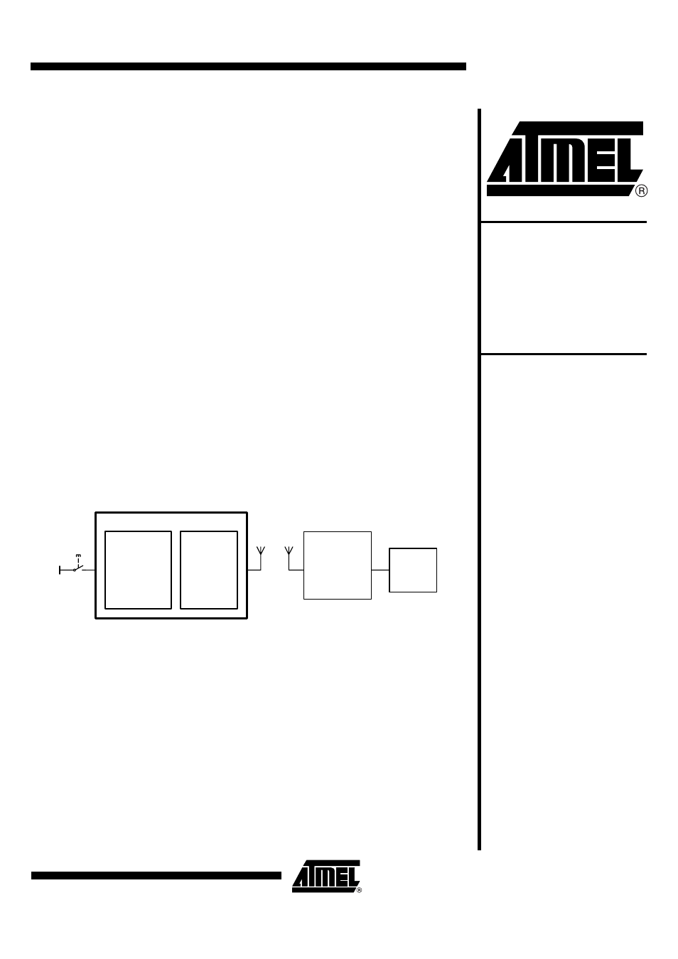
Figure 1.
Application Diagram
Antenna
Micro-
controller
PLL-
Transmitter
ATAR862-8
Keys
UHF ASK/FSK
Receiver
Micro-
controller
Microcontroller
with UHF
ASK/FSK
Transmitter
ATAR862-8
Preliminary
Rev. 4589B–4BMCU–02/03
Document Outline
- Features
- Description
- Pin Configuration
- Pin Description: RF Part
- Pin Description: Microcontroller Part
- UHF ASK/FSK Transmitter Block
- Features
- Description
- General Description
- Functional Description
- Absolute Maximum Ratings
- Thermal Resistance
- Electrical Characteristics
- Microcontroller Block
- Features
- Description
- Introduction
- MARC4 Architecture General Description
- Components of MARC4 Core
- Master Reset
- Voltage Monitor
- Clock Generation
- Power-down Modes
- Peripheral Modules
- Bi-directional Ports
- Timer 3
- Features
- Timer/Counter Modes
- Timer 3 – Mode 1: Timer/Counter
- Timer 3 – Mode 2: Timer/Counter, External Trigger Restart and External Capture (with T3I Input)
- Timer 3 – Mode 3: Timer/Counter, Internal Trigger Restart and Internal Capture (with TOG2)
- Timer 3 – Mode 4: Timer/Counter
- Timer 3 – Mode 5: Timer/Counter, External Trigger Restart and External Capture (with T3I Input)
- Timer 3 Modulator/Demodulator Modes
- Timer 3 – Mode 6: Carrier Frequency Burst Modulation Controlled by Timer 2 Output Toggle Flip- Fl...
- Timer 3 – Mode 7: Carrier Frequency Burst Modulation Controlled by SSI Internal Output (SO)
- Timer 3 – Mode 8: FSK Modulation with Shift Register Data (SO)
- Timer 3 – Mode 9: Pulse-width Modulation with the Shift Register
- Timer 3 – Mode 10: Manchester Demodulation/ Pulse-width Demodulation
- Timer 3 – Mode 11: Biphase Demodulation
- Timer 3 – Mode 12: Timer/Counter with External Capture Mode (T3I)
- Timer 3 Modulator for Carrier Frequency Burst Modulation
- Timer 3 Demodulator for Biphase, Manchester and Pulse-width-modulated Signals
- Timer 3 Registers
- Timer 3 Mode Register (T3M)
- Timer 3 Control Register 1 (T3C) Write
- Timer 3 Status Register 1 (T3ST) Read
- Timer 3 Clock Select Register (T3CS)
- Timer 3 Compare- and Compare-mode Register
- Timer 3 Compare-Mode Register 1 (T3CM1)
- Timer 3 Compare Mode Register 2 (T3CM2)
- Timer 3 COmpare Register 1 (T3CO1) Byte Write
- Timer 3 COmpare Register 2 (T3CO2) Byte Write
- Timer 3 Capture Register
- Synchronous Serial Interface (SSI)
- Serial Interface Registers
- Combination Modes
- Microcontroller Block
- Absolute Maximum Ratings
- Thermal Resistance
- DC Operating Characteristics
- AC Characteristics
- Crystal Characteristics
- Ordering Information
- Ordering Information
- Package Information
- Table of Contents
