Pin configuration, Pin description: rf part, Atar862-8 – Rainbow Electronics ATAR862-8 User Manual
Page 2
2
ATAR862-8
4589B–4BMCU–02/03
Pin Configuration
Figure 2.
Pinning SSO24
XTAL
VS
GND
ENABLE
NRESET
BP63/T3I
BP20/NTE
BP23
BP41/T2I/VMI
BP42/T2O
BP43/SD/INT3
VSS
ANT1
ANT2
PA_ENABLE
CLK
BP60/T3O
OSC2
OSC1
BP50/INT6
BP52/INT1
BP53/INT1
BP40/SC/INT3
VDD
1
2
3
4
5
6
7
8
9
10
11
12
24
23
22
21
20
19
18
17
16
15
14
13
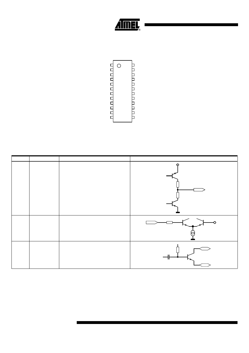
Pin Description: RF Part
Pin
Symbol
Function
Configuration
1
CLK
Clock output signal for microcontroller
The clock output frequency is set by the
crystal to f
XTAL
/4
2
PA_ENABLE
Switches on power amplifier, used for
ASK modulation
3
4
ANT2
ANT1
Emitter of antenna output stage
Open collector antenna output
CLK
VS
100
100
PA_ENABLE
50k
Uref=1.1V
20 µA
ANT1
ANT2
See also other documents in the category Rainbow Electronics Wireless Headsets:
- RC2000 (2 pages)
- Т7023 (12 pages)
- Т7024 (20 pages)
- RC2200 (17 pages)
- RF01 (26 pages)
- RC1090 (17 pages)
- U3741BM (32 pages)
- U3742BM (32 pages)
- RAM01 (7 pages)
- RF22 (92 pages)
- RC1180-MBUS (28 pages)
- RFM01 (8 pages)
- RF12B (36 pages)
- RC1290 (17 pages)
- RC2300-ZNM (1 page)
- RF12 (31 pages)
- T48C862-R3 (107 pages)
- RF02 (24 pages)
- T48C862-R8 (107 pages)
- RFM12 (10 pages)
- U3745BM (29 pages)
- T5744 (19 pages)
- RFM12B (10 pages)
- U2745B (9 pages)
- T48C862-R4 (107 pages)
- RA01 (19 pages)
- T5754 (11 pages)
- U2741B (9 pages)
- RFM02 (8 pages)
- RC2100 (22 pages)
- RF модули диапазона ISM (4 pages)
- T5761 (35 pages)
- BTM -17х (5 pages)
- ATA8401 (12 pages)
- BTM -22х (7 pages)
- AT86RF231 (180 pages)
- ATA5575M1 (7 pages)
- AT88RF1354 (50 pages)
- ATA5812 (90 pages)
- AT86RF401 (50 pages)
- AT76C551 (77 pages)
- BTM -250 (6 pages)
- AT75C310 (132 pages)
- AT75C320 (13 pages)
- BTM -140 (6 pages)