4 register description, 1 mcucr – mcu control register, 2 porta – port a data register – Rainbow Electronics ATtiny43U User Manual
Page 78: 3 ddra – port a data direction register, 4 pina – port a input pins address, 5 portb – port b data register, 6 ddrb – port b data direction register, 7 pinb – port binput pins address, Attiny43u
78
8048B–AVR–03/09
ATtiny43U
11.4
Register Description
11.4.1
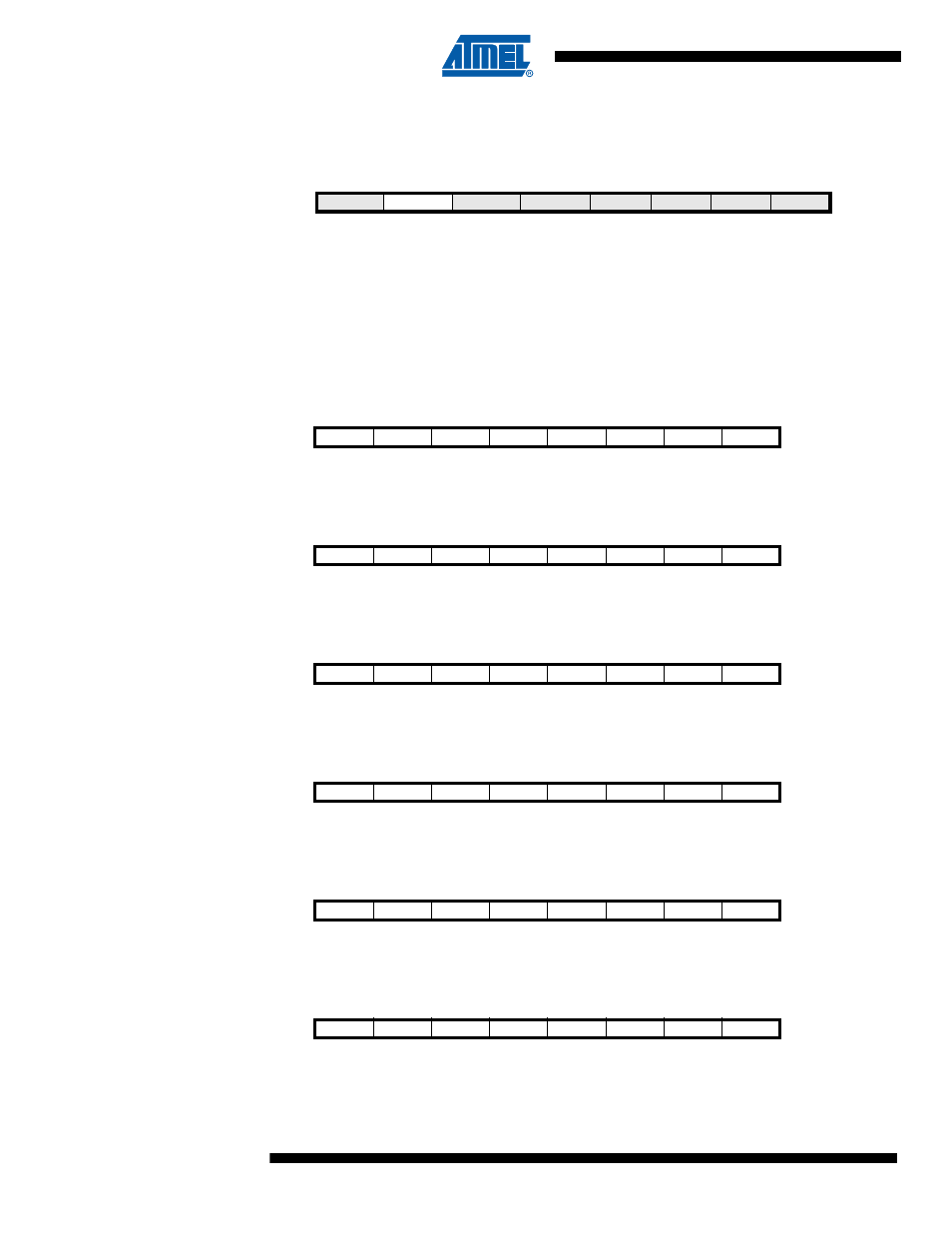
MCUCR – MCU Control Register
• Bit 6 – PUD: Pull-up Disable
When this bit is written to one, the pull-ups in the I/O ports are disabled even if the DDxn and
PORTxn Registers are configured to enable the pull-ups ({DDxn, PORTxn} = 0b01). See
for more details about this feature.
11.4.2
PORTA – Port A Data Register
11.4.3
DDRA – Port A Data Direction Register
11.4.4
PINA – Port A Input Pins Address
11.4.5
PORTB – Port B Data Register
11.4.6
DDRB – Port B Data Direction Register
11.4.7
PINB – Port BInput Pins Address
Bit
7
6
5
4
3
2
1
0
0x35 (0x55)
BODS
PUD
SE
SM1
SM0
BODSE
ISC01
ISC00
MCUCR
Read/Write
R/W
R/W
R/W
R/W
R/W
R/W
R/W
R/W
Initial Value
0
0
0
0
0
0
0
0
Bit
7
6
5
4
3
2
1
0
PORTA7
PORTA6
PORTA5
PORTA4
PORTA3
PORTA2
PORTA1
PORTA0
PORTA
Read/Write
R/W
R/W
R/W
R/W
R/W
R/W
R/W
R/W
Initial Value
0
0
0
0
0
0
0
0
Bit
7
6
5
4
3
2
1
0
DDA7
DDA6
DDA5
DDA4
DDA3
DDA2
DDA1
DDA0
DDRA
Read/Write
R/W
R/W
R/W
R/W
R/W
R/W
R/W
R/W
Initial Value
0
0
0
0
0
0
0
0
Bit
7
6
5
4
3
2
1
0
PINA7
PINA6
PINA5
PINA4
PINA3
PINA2
PINA1
PINA0
PINA
Read/Write
R/W
R/W
R/W
R/W
R/W
R/W
R/W
R/W
Initial Value
N/A
N/A
N/A
N/A
N/A
N/A
N/A
N/A
Bit
7
6
5
4
3
2
1
0
PORTB7
PORTB6
PORTB5
PORTB4
PORTB3
PORTB2
PORTB1
PORTB0
PORTB
Read/Write
R/W
R/W
R/W
R/W
R/W
R/W
R/W
R/W
Initial Value
0
0
0
0
0
0
0
0
Bit
7
6
5
4
3
2
1
0
DDB7
DDB6
DDB5
DDB4
DDB3
DDB2
DDB1
DDB0
DDRB
Read/Write
R/W
R/W
R/W
R/W
R/W
R/W
R/W
R/W
Initial Value
0
0
0
0
0
0
0
0
Bit
7
6
5
4
3
2
1
0
PINB7
PINB6
PINB5
PINB4
PINB3
PINB2
PINB1
PINB0
PINB
Read/Write
R/W
R/W
R/W
R/W
R/W
R/W
R/W
R/W
Initial Value
N/A
N/A
N/A
N/A
N/A
N/A
N/A
N/A