Pin configurations, 1 pin descriptions, 1 vcc – Rainbow Electronics ATtiny43U User Manual
Page 2: 2 gnd, 3 port a (pa7:pa0), Attiny43u, Qfn/mlf top view soic
2
8048B–AVR–03/09
ATtiny43U
1.
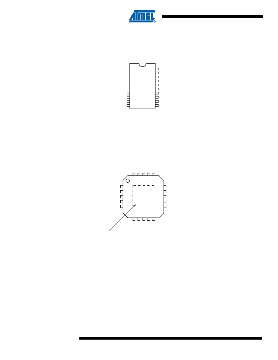
Pin Configurations
Figure 1-1.
Pinout of ATtiny43U
1.1
Pin Descriptions
1.1.1
V
CC
Supply voltage.
1.1.2
GND
Ground.
1.1.3
Port A (PA7:PA0)
Port A is a 8-bit bi-directional I/O port with internal pull-up resistors (selected for each bit). The
Port A output buffers have symmetrical drive characteristics with both high sink and source
(T0/PCINT8) PB0
(OC0A/PCINT9) PB1
(OC0B/PCINT10) PB2
(T1/CLKO/PCINT11) PB3
(DI/OC1A/PCINT12) PB4
(DO/OC1B/PCINT13) PB5
(USCK/SCL/PCINT14) PB6
(INT0/PCINT15) PB7
VCC
GND
20
19
18
17
16
15
14
13
12
11
1
2
3
4
5
6
7
8
9
10
PA7 (RESET/dW/PCINT7)
PA6 (CLKI/PCINT6)
PA5 (AIN1/PCINT5)
PA4 (AIN0/PCINT4)
PA3 (ADC3/PCINT3)
PA2 (ADC2/PCINT2)
PA1 (ADC1/PCINT1)
PA0 (ADC0/PCINT0)
VBAT
LSW
QFN/MLF Top View
SOIC
NOTE: Bottom pad should
be Soldered to ground.
1
2
3
4
5
15
14
13
12
11
20
19
18
17
16
6
7
8
9
10
(OC0B/PCINT9) PB2
(T1/CLKO/PCINT11) PB
3
(DI/OC1A/PCINT12)
PB4
(DO/OC1B/PCINT13)
PB5
(USCK/SCL/PCINT14)
PB6
PA4 (AIN0/
PCINT4
)
PA3 (ADC3/
PCINT3
)
PA2 (ADC2/
PCINT2
)
PA1 (ADC1/
PCINT1
)
PA0 (ADC0/
PCINT0
)
(INT0/PCINT15)
PB7
VCC
GND
LSW
VBA
T
PB1
(OC0A/PCINT9)
PB0
(T0/PCINT8)
P
A7
(RESET/dW/PCINT7)
P
A6 (CLKI)
P
A5 (AIN1/PCINT5)