Power supply and on-chip boost converter, 1 overview, Attiny43u – Rainbow Electronics ATtiny43U User Manual
Page 36

36
8048B–AVR–03/09
ATtiny43U
8.
Power Supply and On-Chip Boost Converter
In order to work properly microcontrollers typically require a supply voltage level that can not be
provided by battery packs of less than two or three battery cells. This constraint adds to size,
cost and complexity of the design. The integrated boost converter of ATtiny43U bridges the gap
between minimum supply voltage of the device and typical output voltages of single-cell stan-
dard, alkaline, Lithium, NiCd or NiMH batteries. The boost converter enables the device to be
powered from a source with a supply voltage well below 1V.
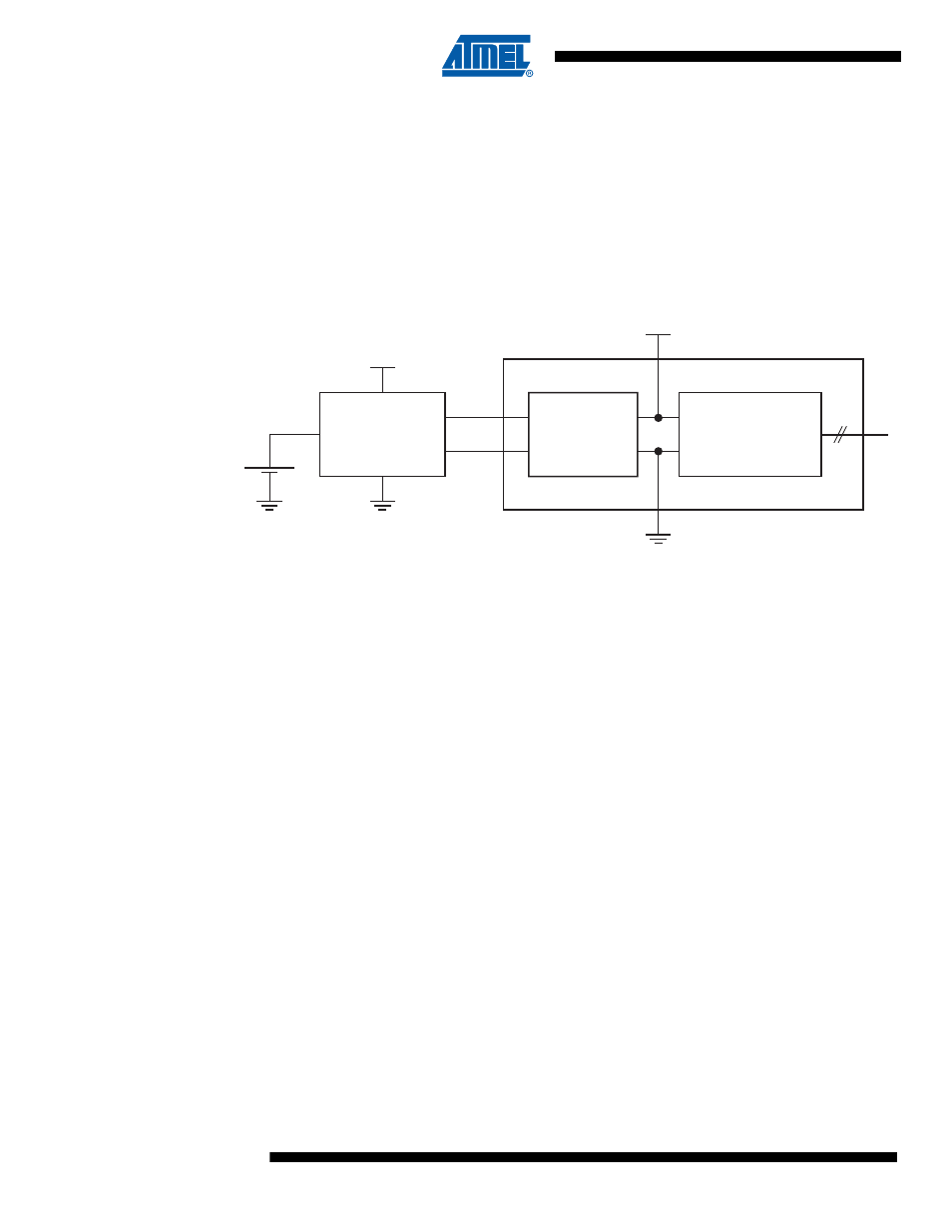
A block diagram illustrating the use of the boost converter is shown in
Figure 8-1.
Block Diagram of Boost Converter Usage.
8.1
Overview
A boost converter is a device that converts a DC voltage to a higher level. The integrated boost
converter of ATtiny43U provides the microcontroller (and its peripherals) with a fixed supply volt-
age, generated from an external supply of lower voltage.
The ATtiny43U boost converter is a switching type, step-up converter that uses an external
inductor, a diode and bypass capacitors. The boost converter is self-sufficient, completely inde-
pendent and does not need any control from the MCU. The converter starts automatically as
soon as there is sufficient voltage at the V
BAT
pin. See
for electrical
characteristics.
The microcontroller starts as soon as the regulated output of the boost converter rises above
power-on and brown-out reset levels (if enabled), as described in section
. After the MCU is released from reset and has started running the application
software can then measure the battery voltage and decide if there is sufficient voltage to con-
tinue operation.
The boost converter continuously switches between storing energy in and draining energy from
the external inductor. During the charge phase the current through the inductor ramps up at a
rate determined by the converter input voltage. During the discharge phase energy stored in the
inductor is released to the load and the current in the inductor ramps down at a rate determined
by the difference between the input and output voltages.
The boost converter requires some external components to operate. See
for component placement. The circuit is completed by inserting an inductor between node VIN
and pin LSW, and a Schottky diode between pins LSW and V
CC
. In addition, an input capacitor
and external bypass capacitor from V
CC
to GND are typically required. See
for more details.
REGULATOR
MCU
EXTERNAL
COMPONENTS
V
BAT
LSW
16
ATtiny43U
I/O
V
CC
GND
VIN
