7 typical applications, 8 characteristics, 9 potential limitations – Rainbow Electronics ATtiny43U User Manual
Page 46: 10 bypassing the boost converter, Typical applica, Attiny43u
46
8048B–AVR–03/09
ATtiny43U
8.7
Typical Applications
A typical use of the boost converter is illustrated in
. Components can be
optimized depending on the type of application.
, below, presents recommendations for
three different types of applications (cost effective, high output current and long battery life). All
values are guidelines, only.
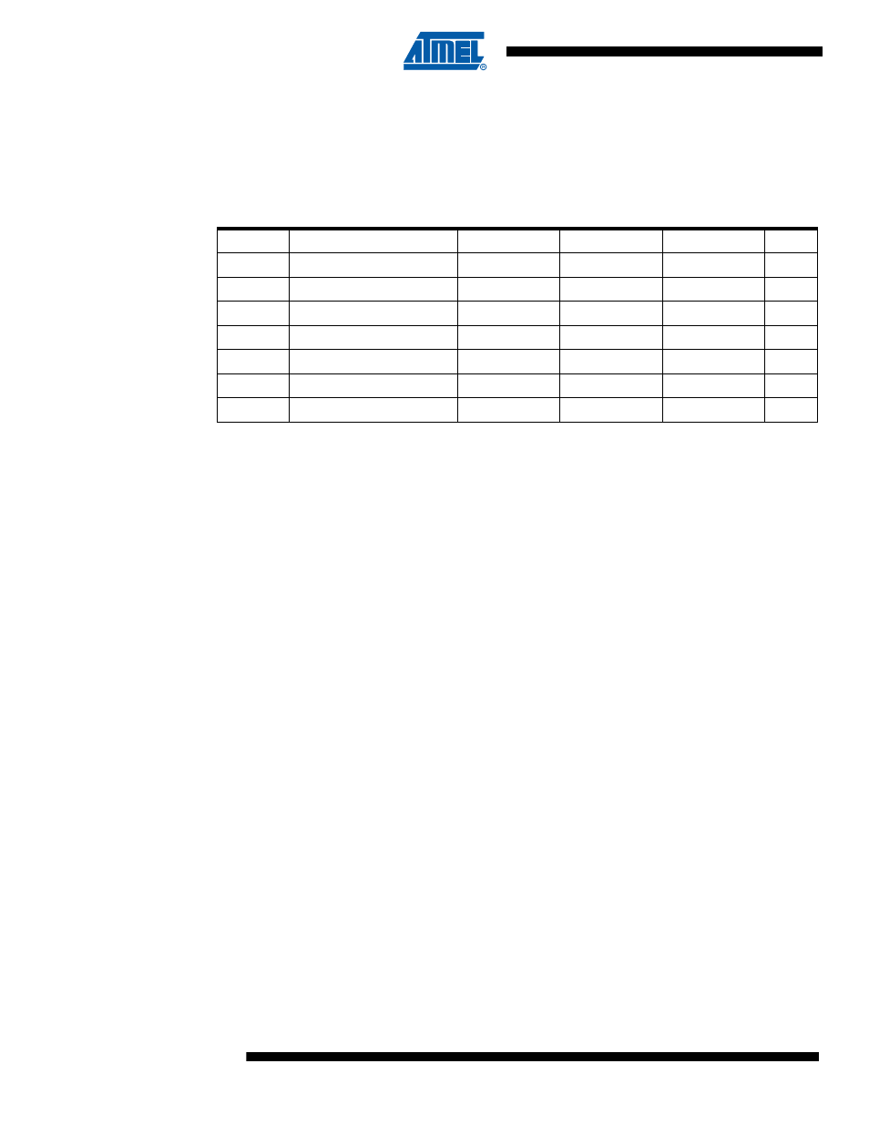
Notes:
1. Low ESR required.
2. High reverse leakage current, increases current consumption.
3. The diode is the largest individual contributor to battery life. The example diode keeps the
boost converter running and maintains a reasonable efficiency level.
4. Depends on internal resistance of power supply.
5. Depends on load current. May not be sufficient for maximum current rating.
8.8
Characteristics
Electrical characteristics of the boost converter are given in
. Typical
characteristics can be found under section
8.9
Potential Limitations
When the device is powered via the boost converter some usage limitiations may apply. For
example, the highest allowed operating frequency of the device depends on supply voltage (see
) and the boost converter output voltage varies within the limits
given in
. This means that if the design allows the boost converter to go
into Active Low Current Mode the supply voltage will drop periodically, affecting the maximum
allowed operating frequency.
Provided the load current remains sufficiently high the boost converter will never enter Active
Low Current Mode and the supply voltage will remain high enough to run the device at higher
frequencies. The boost converter status bit BS can be used to determine if the boost converter is
in Low Current Mode (see
“ADCSRB – ADC Control and Status Register B” on page 47
).
Since the entire device is powered from the boost converter output variations will show in all
peripherals. This means that, for example, high levels of I/O pins may vary with supply voltage.
8.10
Bypassing the Boost Converter
It is possible to bypass and disable the boost converter so that the device can be powered
directly from an external supply. To force the boost converter into Stop Mode, connect pin V
BAT
to ground and provide the device with supply directly to the V
CC
pin. To permanently disable the
Table 8-2.
Recommended Components and Values for Various Designs
Symbol
Component
Cost Effective
High Current
Battery Life
Unit
L
1
Inductor
15
15
µH
D
1
Schottky diode
10MQ100N
10BQ040
R
1
Resistor
680
680
680
Ω
C
1
Input Capacitor
4.7
4.7
µF
C
2
Secondary Input Cap.
100
100
100
nF
C
3
Output Capacitor
22
22
µF
C
4
Secondary Output Cap.
–
22
22
nF