3 speed grades, Attiny43u, Safe operating area – Rainbow Electronics ATtiny43U User Manual
Page 156
156
8048B–AVR–03/09
ATtiny43U
Notes:
1. “Max” means the highest value where the pin is guaranteed to be read as low.
2. Not tested in production.
3. “Min” means the lowest value where the pin is guaranteed to be read as high.
4. Although each I/O port can under steady state (non-transient) conditions sink more than indicated, the sum of all I
OL
currents
may not exceed 60 mA, or the boost converter limits. If I
OL
limits are exceeded the corresponding V
OL
levels can not be guar-
anteed. Pins are not guaranteed to sink currents greater than those listed.
5. Pins PB1, PB2, PB4 and PB5 are high sink I/O pins.
6. Although each I/O port can under steady state (non-transient) conditions source more than indicated, the sum of all I
OH
cur-
rents may not exceed 60 mA, or the boost converter limits. If I
OH
limits are exceeded the corresponding V
OH
levels can not be
guaranteed. Pins are not guaranteed to source currents greater than those listed.
“Boost Converter Characteristics” on page 159
for current consumption of entire device, including boost converter.
20.3
Speed Grades
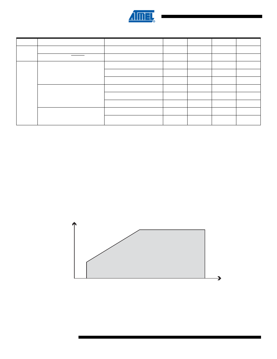
Figure 20-1. Maximum Frequency vs. V
CC
(Boost Converter Disregarded).
R
PU
Pull-up Resistor, I/O Pin
V
CC
=
5.5
V, input low
20
50
k
Ω
Pull-up Resistor, RESET Pin
V
CC
=
5.5
V, input low
30
80
k
Ω
I
CC
Supply Current,
Active Mode,
Without Boost Converter
f = 1MHz, V
CC
= 2V
0.2
0.55
mA
f = 4MHz, V
CC
= 3V
1.3
2.5
mA
f = 8MHz, V
CC
= 5V
4
7
mA
Supply Current,
Idle Mode,
Without Boost Converter
f = 1MHz, V
CC
= 2V
0.04
0.15
mA
f = 4MHz, V
CC
= 3V
0.25
0.6
mA
f = 8MHz, V
CC
= 5V
1.0
2.0
mA
Supply Current,
Power-Down Mode,
Without Boost Converter
WDT enabled, V
CC
= 3V
4.5
10
µA
WDT disabled, V
CC
= 3V
0.35
2
µA
Table 20-1.
DC Characteristics. T
A
= -40
°
C to 85
°
C (Continued)
Symbol
Parameter
Condition
Min.
Typ.
Max.
Units
8 MHz
4 MHz
1.8V
2.7V
5.5V
Safe Operating Area