6 changing channel or reference selection, Figure 16-7, Attiny43u – Rainbow Electronics ATtiny43U User Manual
Page 120
120
8048B–AVR–03/09
ATtiny43U
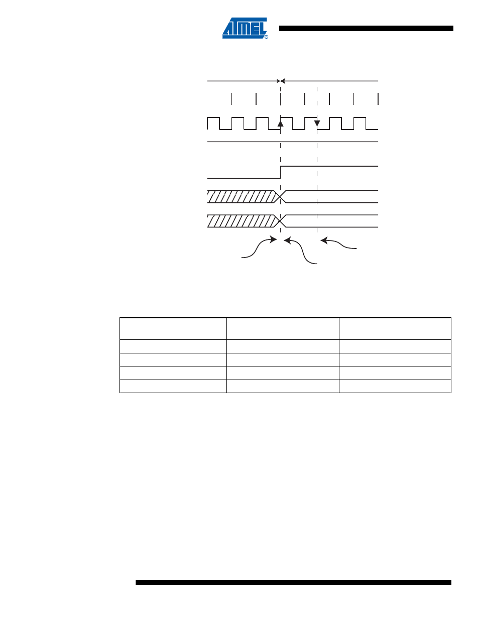
Figure 16-7. ADC Timing Diagram, Free Running Conversion
For a summary of conversion times, see
.
16.6
Changing Channel or Reference Selection
The MUX[2:0] and REFS bits in the ADMUX Register are single buffered through a temporary
register to which the CPU has random access. This ensures that the channels and reference
selection only takes place at a safe point during the conversion. The channel and reference
selection is continuously updated until a conversion is started. Once the conversion starts, the
channel and reference selection is locked to ensure a sufficient sampling time for the ADC. Con-
tinuous updating resumes in the last ADC clock cycle before the conversion completes (ADIF in
ADCSRA is set). Note that the conversion starts on the following rising ADC clock edge after
ADSC is written. The user is thus advised not to write new channel or reference selection values
to ADMUX until one ADC clock cycle after ADSC is written.
If Auto Triggering is used, the exact time of the triggering event can be indeterministic. Special
care must be taken when updating the ADMUX Register, in order to control which conversion
will be affected by the new settings.
Table 16-1.
ADC Conversion Time
Condition
Sample & Hold (Cycles from
Start of Conversion)
Conversion Time (Cycles)
First conversion
13.5
25
Normal conversions
1.5
13
Auto Triggered conversions
2
13.5
Free Running conversion
2.5
14
11
12
13
Sign and MSB of Result
LSB of Result
ADC Clock
ADSC
ADIF
ADCH
ADCL
Cycle Number
1
2
One Conversion
Next Conversion
3
4
Conversion
Complete
Sample & Hold
MUX and REFS
Update