Spi interface, Figure 10. spi write cycle, Figure 11. spi read cycle – Rainbow Electronics MAX14821 User Manual
Page 26
���������������������������������������������������������������� Maxim Integrated Products 26
MAX14821
IO-Link Device Transceiver
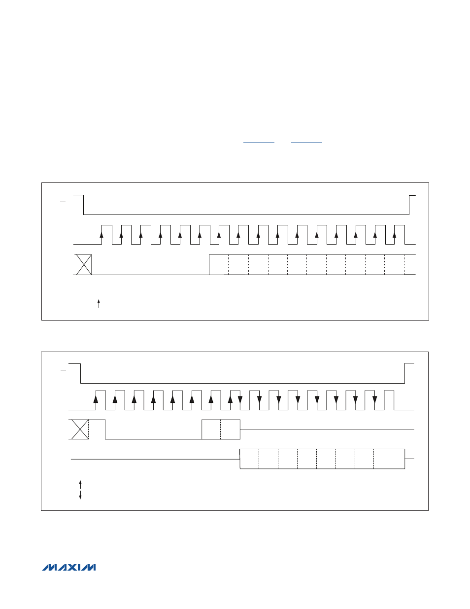
SPI Interface
The device communicates through an SPI-compatible
4-wire serial interface. The interface has three inputs—
clock (SCLK), chip select (CS), and data in (SDI)—and
one output, data out (SDO). The maximum SPI clock rate
for the device is 12MHz. The SPI interface complies with
clock polarity CPOL = 0 and clock phase CPHA = 0 (see
).
The SPI interface is not available when V
5
or V
L
are not
present.
Figure 10. SPI Write Cycle
Figure 11. SPI Read Cycle
R0
D7
D6
D5
D4
D3
D2
D1
D0
SCLK
R_ = REGISTER ADDRESS
D_ = DATA BIT
= CLOCK EDGE WHEN LOGIC IS LATCHED
SDI
W
0
0
0
0
0
R1
CS
SDI
SDO
SCLK
R
R1
R0
0
0
0
0
0
CS
D7
D6
D5
D4
D3
D2
D1
D0
R_ = REGISTER ADDRESS
D_ = DATA BIT
= CLOCK EDGE WHEN LOGIC IS LATCHED
= CLOCK EDGE AT WHICH LOGIC IS WRITTEN
- MAX12005 (14 pages)
- MAX7058 (14 pages)
- MAX9995 (13 pages)
- MAX7034 (13 pages)
- MAX7033 (16 pages)
- MAX9476 (8 pages)
- MAX9486 (8 pages)
- MAX9489 (11 pages)
- MAX9491 (11 pages)
- DS2130Q (22 pages)
- DS21458 (270 pages)
- DS3131 (174 pages)
- DS26502 (125 pages)
- DS2153Q (48 pages)
- DS26503 (123 pages)
- DS2186 (11 pages)
- DS1842A (6 pages)
- DS3134 (203 pages)
- DS1876 (69 pages)
- DS1874 (88 pages)
- DS31256 (181 pages)
- DS2141A (35 pages)
- DS3184 (13 pages)
- DS2154 (69 pages)
- DS26504 (128 pages)
- DS3164 (12 pages)
- DS1852 (25 pages)
- DS2181A (32 pages)
- DS2151Q (46 pages)
- DS1843 (8 pages)
- DS2165Q (17 pages)
- DS3170 (233 pages)
- DS2180A (36 pages)
- DS2172 (20 pages)
- DS2152 (79 pages)
- DS1841 (16 pages)
- DS2182A (22 pages)
- DS2143Q (40 pages)
- DS2132A_Q (17 pages)
- DS1862 (42 pages)
- DS26519 (310 pages)
- DS2188 (11 pages)
- DS1875 (92 pages)
- DS33M33 (20 pages)