Pin/bump configurations, Pin/bump descriptions, Pin/bump configurations pin/bump descriptions – Rainbow Electronics MAX14821 User Manual
Page 14
���������������������������������������������������������������� Maxim Integrated Products 14
MAX14821
IO-Link Device Transceiver
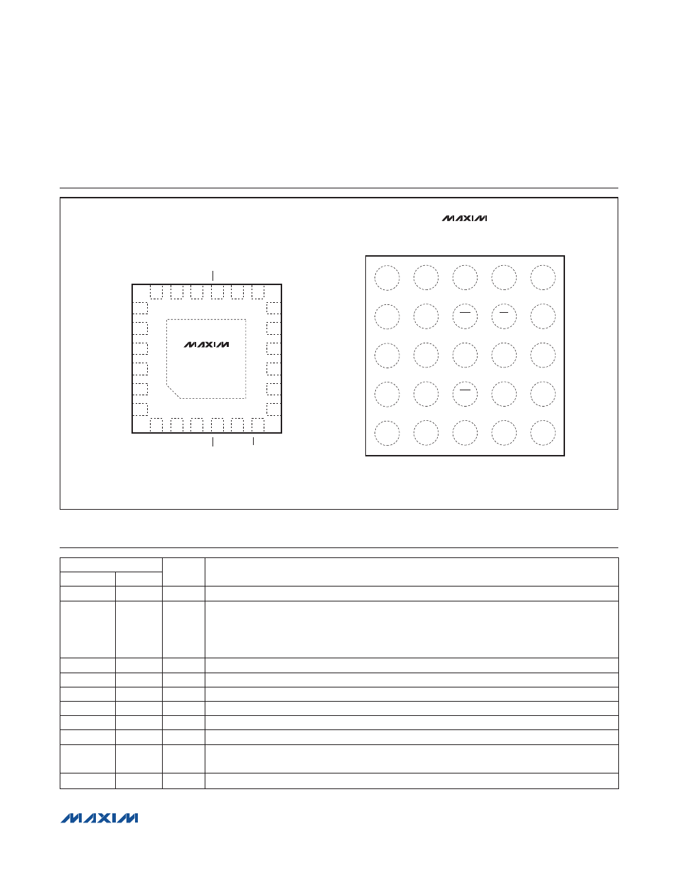
Pin/Bump Configurations
Pin/Bump Descriptions
PIN
NAME
FUNCTION
TQFN-EP
WLP
1
A2
LDOIN
5V Linear Regulator Input. Bypass LDOIN to GND with a 0.1FF ceramic capacitor.
2
A3
V
5
5V Power-Supply Input and 5V Linear Regulator Output. Bypass V
5
to GND with a 0.1FF
ceramic capacitor for 10mA load capability. Add the recommended compensation network
to increase the source capability to 30mA. See the 5V and 3.3V Linear Regulators section for
more information.
3
A4
LDO33
3.3V Linear Regulator Output. Bypass LDO33 to GND with a 1FF ceramic capacitor.
4
B3
IRQ
Active-Low Interrupt Request Output. IRQ is a push-pull output referenced to V
L
.
5
A5
SCLK
SPI Clock Input
6
B4
CS
Active-Low SPI Chip-Select Input
7
B5
SDO
SPI Serial-Data Output
8
C4
SDI
SPI Serial-Data Input
9
C5
V
L
Logic-Level Supply Input. V
L
defines the logic levels on all the logic inputs and outputs.
Bypass V
L
to GND with a 0.1FF ceramic capacitor.
10
C3
I.C.
Internally Connected. Connect to V
L
or leave unconnected.
23
24
22
21
8
7
9
V
5
IRQ
SCLK
CS
10
LDOIN
LI
WU
RX
UV
TXEN
1
2
DO
4
5
6
17
18
16
14
13
V
CC
V
P
I.C.
V
L
SDI
SDO
*EP
*CONNECT EXPOSED PAD TO GND.
LDO33
LO
3
15
C/Q
20
11 TXQ
GND
19
12 TXC
DI
TQFN
TOP VIEW
+
MAX14821
MAX14821
TOP VIEW
(BUMP SIDE DOWN)
A
B
C
D
WLP
E
1
2
3
4
V
CC
LDOIN
V
5
LDO33
SCLK
C/Q
V
P
IRQ
SDO
GND
GND
I.C.
SDI
V
L
DO
UV
TXC
TXQ
DI
LI
LO
RX
TXEN
5
+
CS
WU