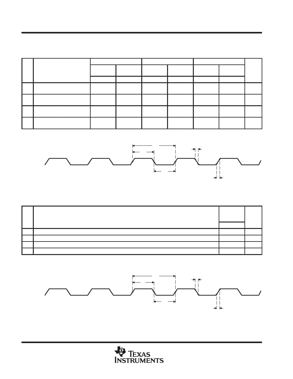
Adv ance informa tion, See figure 8), Timing requirements for xclkin – Texas Instruments TMS320C6202 User Manual
Page 30: See figure 9)

TMS320C6202
FIXED-POINT DIGITAL SIGNAL PROCESSOR
SPRS072B – AUGUST 1998 – REVISED AUGUST 1999
30
POST OFFICE BOX 1443
•
HOUSTON, TEXAS 77251–1443
INPUT AND OUTPUT CLOCKS
timing requirements for CLKIN
†
(see Figure 8)
’C6202-200
’C6202-233
’C6202-250
NO.
CLKMODE
= x4
CLKMODE
= x1
CLKMODE
= x4
CLKMODE
= x1
CLKMODE
= x4
CLKMODE
= x1
UNIT
MIN
MAX
MIN
MAX
MIN
MAX
MIN
MAX
MIN
MAX
MIN
MAX
1
tc(CLKIN)
Cycle time,
CLKIN
20
5
17.2
4.3
16
4
ns
2
tw(CLKINH)
Pulse duration,
CLKIN high
8
2.25
6.9
1.9
6.4
1.8
ns
3
tw(CLKINL)
Pulse duration,
CLKIN low
8
2.25
6.9
1.9
6.4
1.8
ns
4
tt(CLKIN)
Transition time,
CLKIN
5
0.6
5
0.6
5
0.6
ns
† The reference points for the rise and fall transitions are measured at 20% and 80%, respectively, of VIH.
CLKIN
1
2
3
4
4
Figure 8. CLKIN Timings
timing requirements for XCLKIN
†‡
(see Figure 9)
NO.
’C6202-200
’C6202-233
’C6202-250
UNIT
MIN
MAX
1
tc(XCLKIN)
Cycle time, XCLKIN
4P
ns
2
tw(XCLKINH) Pulse duration, XCLKIN high
1.8P
ns
3
tw(XCLKINL)
Pulse duration, XCLKIN low
1.8P
ns
4
tt(XCLKIN)
Transition time, XCLKIN
0.6
ns
† The reference points for the rise and fall transitions are measured at 20% and 80%, respectively, of VIH.
‡ P = 1/CPU clock frequency in nanoseconds (ns).
XCLKIN
1
2
3
4
4
Figure 9. XCLKIN Timings
ADV
ANCE INFORMA
TION
