Texas Instruments MSC1210 User Manual
Page 32

Internal RAM
2-6
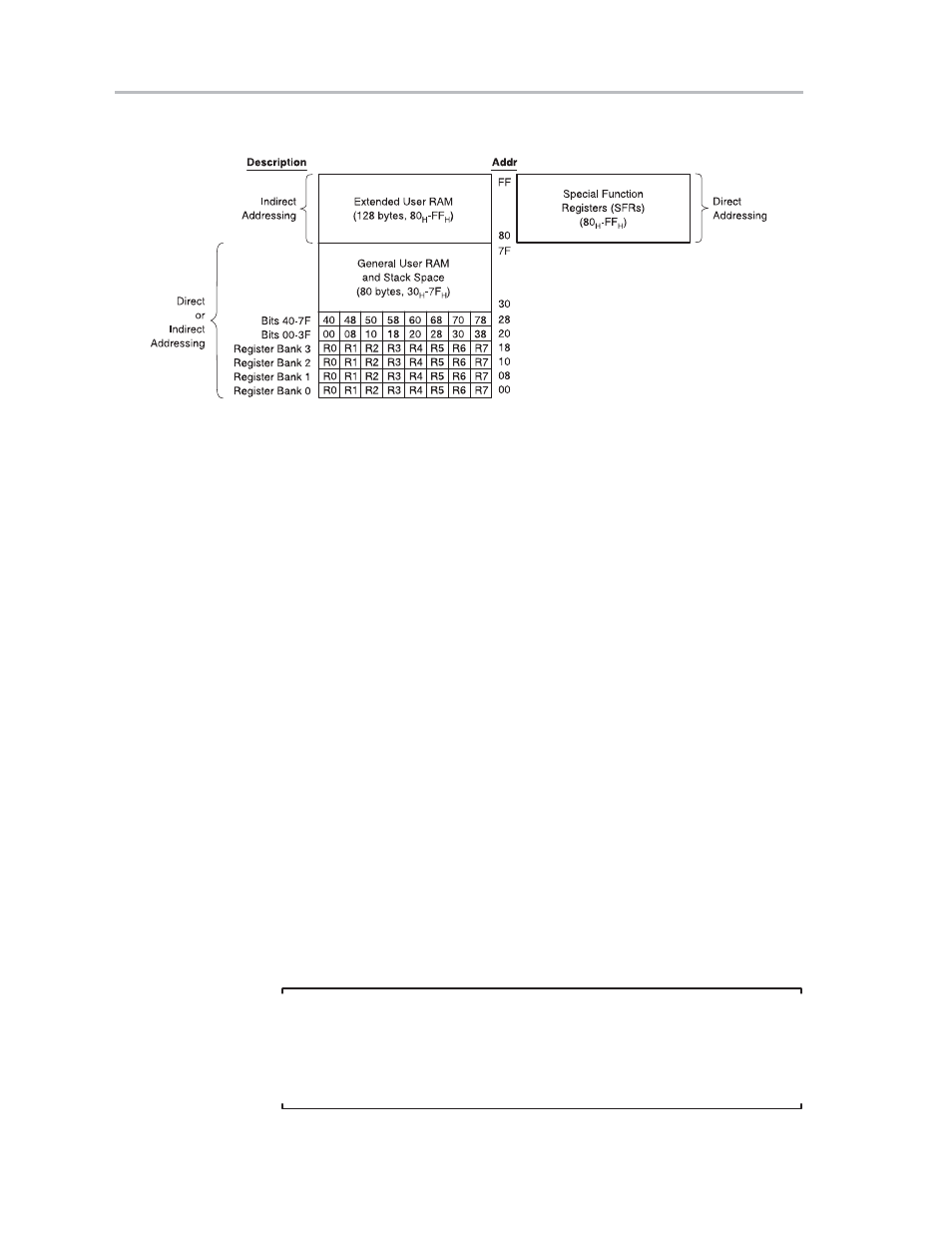
Figure 2−2. MSC1210 Memory Map Register Bank.
2.4
Internal RAM
As shown in Figure 2−2, the MSC1210 has a bank of 256 bytes of internal
RAM. This internal RAM is found on-chip within the IC, so it is the fastest RAM
available and is also the most flexible in terms of reading, writing, and modify-
ing its contents. internal RAM is volatile, so when the MSC1210 is powered up,
the contents of this memory bank is random.
The 256 bytes of internal RAM are subdivided as shown in the memory map
of Figure 2−2. The first eight bytes (00
H−
07
H
) are register bank 0. By manipu-
lating certain SFRs, a program may choose to use register banks 0, 1, 2, or
3. These alternative register banks are located in internal RAM at addresses
08
H
through 1F
H
. Register banks are described in greater detail in chapters
3 and 4. For now it is sufficient to know that they reside in and are part of inter-
nal RAM.
Bit memory also resides in and is part of internal RAM. Bit memory will be de-
scribed more in section 2.4.3, but for now just keep in mind that bit memory
actually resides in internal RAM at addresses 20
H
through 2F
H
.
The 208 bytes remaining of internal RAM, from addresses 30
H
through FF
H
,
may be used by user variables that need to be accessed frequently or at
high-speed. This area is also used by the microcontroller as a storage area for
the operating stack. This fact limits the MSC1210 stack because, as illustrated
in the memory map of Figure 2−2, the area reserved for the stack is only 208
bytes—and usually it is less because these 208 bytes have to be shared
between the stack and user variables.
Note:
Internal RAM addresses 00
H
through 7F
H
may be accessed either via direct
addressing or indirect addressing, whereas internal RAM addresses 80
H
through FF
H
may only be accessed via indirect addressing. This will be dis-
cussed completely in Chapter 5, Addressing Modes.
