2 internal memory spare area assignment, Flex-muxonenand4g(kfm4gh6q4m-debx) – Samsung FLEX-MUXONENAND KFN8GH6Q4M User Manual
Page 30
Flex-MuxOneNAND4G(KFM4GH6Q4M-DEBx)
- 30 -
FLASH MEMORY
Flex-MuxOneNAND8G(KFN8GH6Q4M-DEBx)
Flex-MuxOneNAND16G(KFKAGH6Q4M-DEBx)
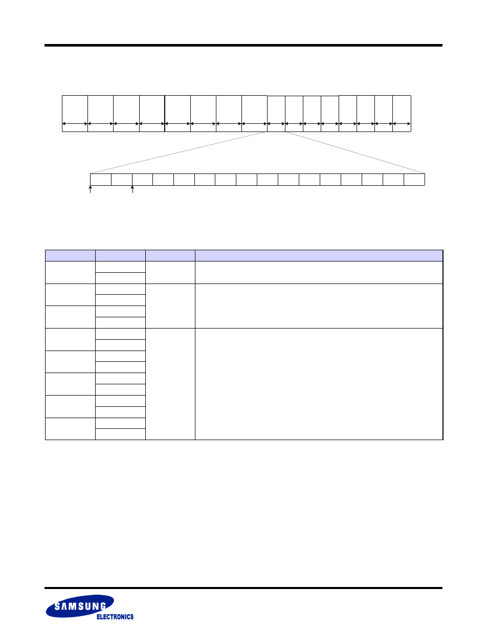
2.7.2 Internal Memory Spare Area Assignment
The figure below shows the assignment of the spare area in the Internal Memory NAND Array.
Spare Area Assignment in the Internal Memory NAND Array Information
Word
Byte
Note
Description
1
LSB
1
Invalid Block information in 1st and 2nd page of an invalid block
MSB
2
LSB
2
Managed by internal ECC logic for Logical Sector Number area
MSB
3
LSB
MSB
4
LSB
3
4bit ECC parity values
MSB
5
LSB
MSB
6
LSB
MSB
7
LSB
MSB
8
LSB
MSB
Spare
area
8W
{
1
st
W
LSB
MSB
LSB
MSB
{
2
nd
W
LSB
MSB
{
3
rd
W
LSB
MSB
{
4
th
W
LSB
MSB
{
5
th
W
LSB
MSB
{
6
th
W
LSB
MSB
{
7
th
W
LSB
MSB
{
8
th
W
LSB
MSB
Note1 Note1 Note2 Note2 Note2 Note2 Note3 Note3 Note3 Note3 Note3 Note3
Note3 Note3 Note3
Note3
Main
area
256W
Main
area
256W
Main
area
256W
Main
area
256W
Main
area
256W
Main
area
256W
Main
area
256W
Main
area
256W
Spare
area
8W
Spare
area
8W
Spare
area
8W
Spare
area
8W
Spare
area
8W
Spare
area
8W
Spare
area
8W