11 program operation timing, Flex-muxonenand4g(kfm4gh6q4m-debx) – Samsung FLEX-MUXONENAND KFN8GH6Q4M User Manual
Page 122
Flex-MuxOneNAND4G(KFM4GH6Q4M-DEBx)
- 122 -
FLASH MEMORY
Flex-MuxOneNAND8G(KFN8GH6Q4M-DEBx)
Flex-MuxOneNAND16G(KFKAGH6Q4M-DEBx)
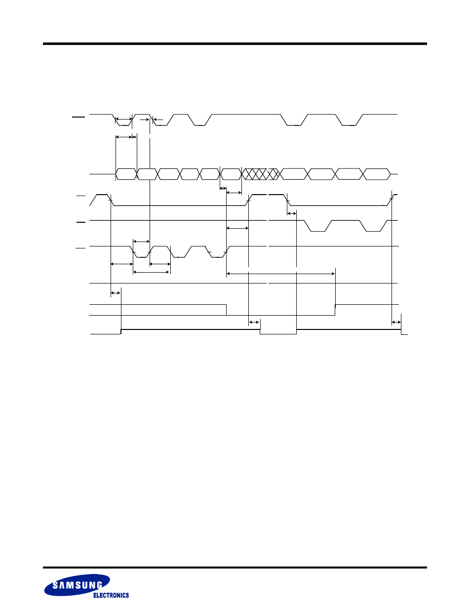
6.11 Program Operation Timing
See AC Characteristics Table 5.7 and Table 5.9
NOTE :
1) AA = Address of address register
CA = Address of command register
PCD = Program Command
PMA = Address of memory to be programmed
BA = Address of BufferRAM to write the data
BD = Program Data
SA = Address of status register
2) “In progress” and “complete” refer to status register
3) Status reads in this figure is asynchronous read, but status read in synchronous mode is also supported.
Program Command Sequence (last two cycles)
WE
CE
CLK
t
DS
t
DH
t
CH
t
WPL
t
CS
t
WPH
t
WC
SA
SA
In
Progress
Completed
AA
OE
Read Status Data
V
IL
AVD
BA
CA
PCD
PMA
BD
t
AAVDH
t
AAVDS
INT
t
AVDP
t
WEA
t
CER
A/DQ0:
A/DQ15
RDY
Hi-Z
t
CER
t
CEZ
bit
t
CEZ
≈
≈
≈
≈
≈
≈
t
PGM1 or tPGM2