6 phase locked loop timing, 7 oscillator parameters, Table 10-14 – Freescale Semiconductor 56F8122 User Manual
Page 110: Table 10-14 pll timing, Table 10-15 crystal oscillator parameters
56F8322 Techncial Data, Rev. 10.0
110
Freescale Semiconductor
Preliminary
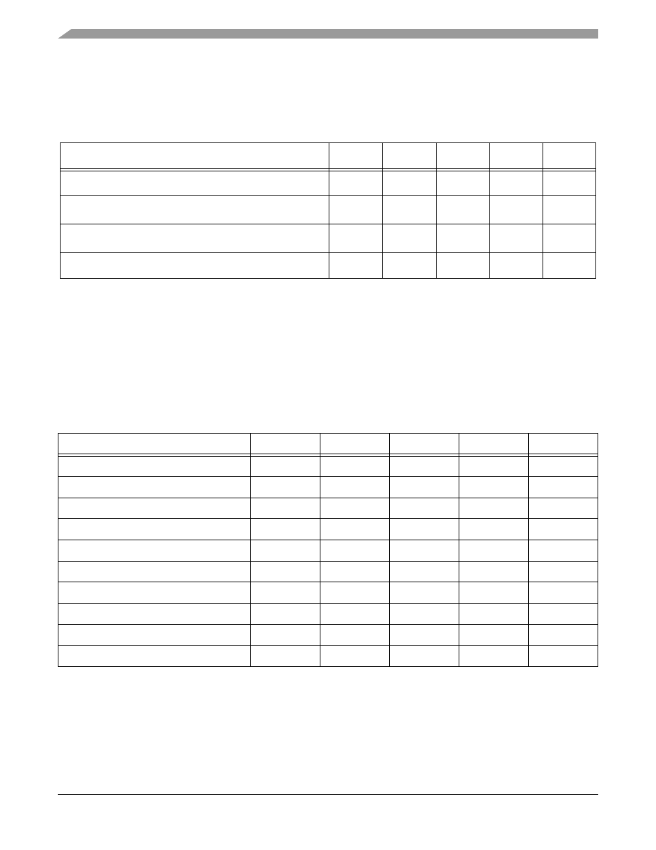
10.6 Phase Locked Loop Timing
10.7 Oscillator Parameters
Table 10-14 PLL Timing
Characteristic
Symbol
Min
Typ
Max
Unit
External reference crystal frequency for the PLL
1
1. An externally supplied reference clock should be as free as possible from any phase jitter for the PLL to work
correctly. The PLL is optimized for 8MHz input crystal.
f
osc
4
8
8
MHz
PLL output frequency
2
(f
OUT
)—56F8322
2. ZCLK may not exceed 60MHz. For additional information on ZCLK and (f
OUT
/2), please refer to the OCCS chapter in the
56F8300 Peripheral User Manual.
f
op
160
—
260
MHz
PLL output frequency
2
(f
OUT
)—56F8122
f
op
160
—
160
MHz
PLL stabilization time
3
-40
°
to +125
°
C
3. This is the minimum time required after the PLL set up is changed to ensure reliable operation.
t
plls
—
1
10
ms
Table 10-15 Crystal Oscillator Parameters
Characteristic
Symbol
Min
Typ
Max
Unit
Crystal Start-up time
T
CS
4
5
10
ms
Resonator Start-up time
T
RS
0.1
0.18
1
ms
Crystal ESR
R
ESR
—
—
120
ohms
Crystal Peak-to-Peak Jitter
T
D
70
—
250
ps
Crystal Min-Max Period Variation
T
PV
0.12
—
1.5
ns
Resonator Peak-to-Peak Jitter
T
RJ
—
—
300
ps
Resonator Min-Max Period Variation
T
RP
—
—
300
ps
Bias Current, high-drive mode
I
BIASH
—
250
290
µ
A
Bias Current, low-drive mode
I
BIASL
—
80
110
µ
A
Quiescent Current, power-down mode
I
PD
—
0
1
µ
A