Figure 1-2 – Freescale Semiconductor 56F8122 User Manual
Page 11
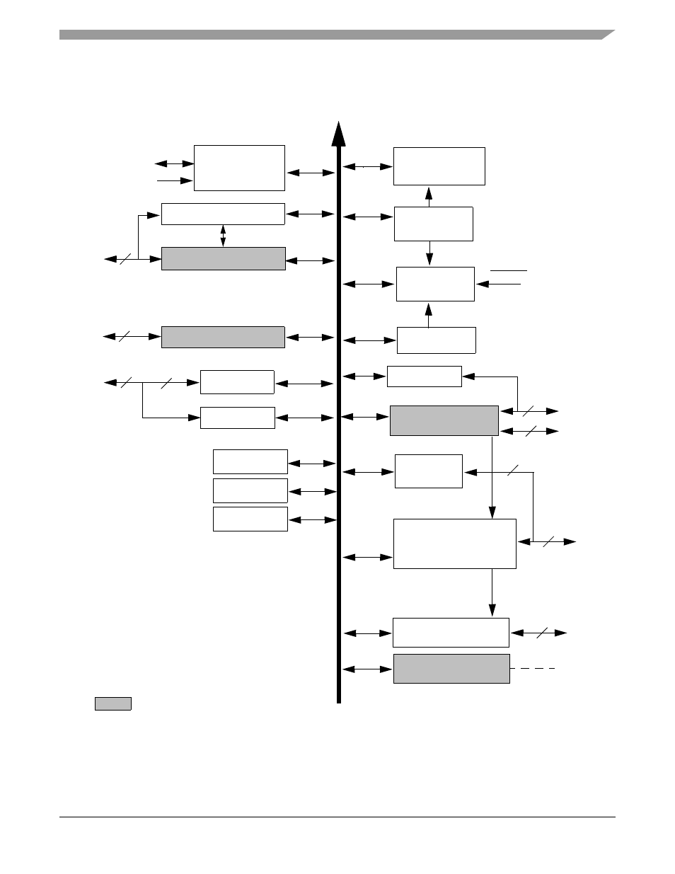
Architecture Block Diagram
56F8322 Technical Data, Rev. 10.0
Freescale Semiconductor
11
Preliminary
Figure 1-2 Peripheral Subsystem
IPBus
Timer A
SPI 0
ADCA
2
6
SPI 1
GPIO A
4
Interrupt
Controller
To/From IPBus Bridge
PWMA
SCI 0
3
System POR
Low-Voltage Interrupt
COP Reset
COP
RESET
Quadrature Decoder 0
4
GPIO B
GPIO C
FlexCAN
SCI 1
4
TEMP_SENSE
CLKGEN
(OSC/PLL)
(ROSC)
POR & LVI
SIM
2
ch2i
ch2o
Timer C
The dotted line on Temperature Sense signifies the
pad-to-pad bond between TEMP_SENSE and
ANA7 on the 56F8322
2
2
SYNC Output
Not available on the 56F8122 device.
This manual is related to the following products: