Figure 12-26, Figure 12-26. pwm disabling scheme – Freescale Semiconductor MC68HC908MR32 User Manual
Page 138
Pulse-Width Modulator for Motor Control (PWMMC)
MC68HC908MR32 • MC68HC908MR16 Data Sheet, Rev. 6.1
138
Freescale Semiconductor
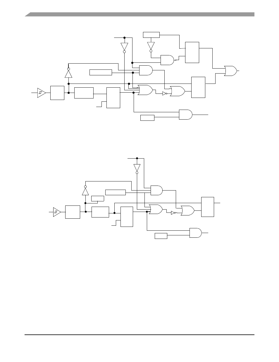
Figure 12-26. PWM Disabling Scheme
FINT2
CYCLE START
LOGIC HIGH FOR FAULT
BANK X
FMODE2
DISX
CLEAR BY WRITING 1 TO FTACK4
INTERRUPT REQUEST
SHOT
S
Q
R
S
Q
R
S
Q
R
ONE
FPIN2
FFLAG2
MANUAL
MODE
AUTO
MODE
SOFTWARE X DISABLE
FAULT PIN 2 DISABLE
The example is of fault pin 2 with DISX. Fault pin 4 with DISY is logically similar and affects BANK Y disable.
Note:
In manual mode (FMODE = 0), faults 2 and 4 may be cleared only if a logic level low at the input of the fault
pin is present.
FAULT
PIN2
DISABLE
TWO
SAMPLE
FILTER
FAULT
PIN1
FINT1
CYCLE START
LOGIC HIGH FOR FAULT
BANK X DISABLE
FMODE1
CLEAR BY WRITING 1 TO FTACK1
INTERRUPT REQUEST
TWO
SHOT
S
Q
R
S
Q
R
SAMPLE
FILTER
ONE
FFLAG1
MANUAL
MODE
AUTO
MODE
FAULT PIN 1 DISABLE
The example is of fault pin 1. Fault pin 3 is logically similar and affects BANK Y disable.
Note:
In manual mode (FMODE = 0), faults 1 and 3 may be cleared regardless of the logic level at the input of the fault pin.
FPIN1