Freescale Semiconductor MC68HC908MR32 User Manual
Page 30
Memory
MC68HC908MR32 • MC68HC908MR16 Data Sheet, Rev. 6.1
30
Freescale Semiconductor
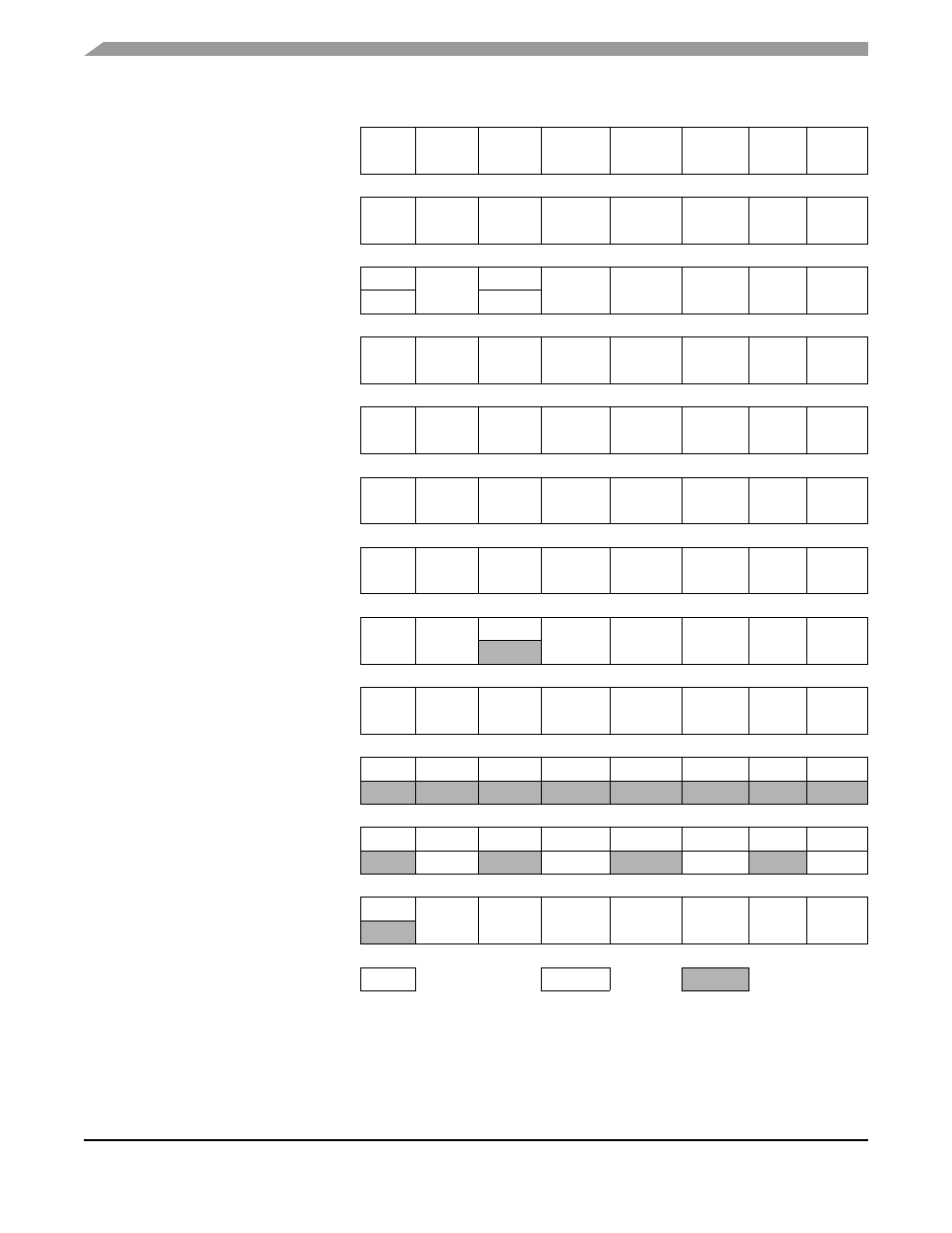
$001A
TIMA Channel 2 Register High
(TACH2H)
Read:
Bit 15
Bit 14
Bit 13
Bit 12
Bit 11
Bit 10
Bit 9
Bit 8
Write:
Reset:
Indeterminate after reset
$001B
TIMA Channel 2 Register Low
(TACH2L)
Read:
Bit 7
Bit 6
Bit 5
Bit 4
Bit 3
Bit 2
Bit 1
Bit 0
Write:
Reset:
Indeterminate after reset
$001C
TIMA Channel 3 Status/Control
Register (TASC3)
Read:
CH3F
CH3IE
0
MS3A
ELS3B
ELS3A
TOV3
CH3MAX
Write:
0
R
Reset:
0
0
0
0
0
0
0
0
$001D
TIMA Channel 3 Register High
(TACH3H)
Read:
Bit 15
Bit 14
Bit 13
Bit 12
Bit 11
Bit 10
Bit 9
Bit 8
Write:
Reset:
Indeterminate after reset
$001E
TIMA Channel 3 Register Low
(TACH3L)
Read:
Bit 7
Bit 6
Bit 5
Bit 4
Bit 3
Bit 2
Bit 1
Bit 0
Write:
Reset:
Indeterminate after reset
$001F
Configuration Register
(CONFIG)
Read:
EDGE
BOTNEG
TOPNEG
INDEP
LVIRST
LVIPWR
STOPE
COPD
Write:
Reset:
0
0
0
0
1
1
0
0
$0020
PWM Control Register 1
(PCTL1)
Read:
DISX
DISY
PWMINT
PWMF
ISENS1
ISENS0
LDOK
PWMEN
Write:
Reset:
0
0
0
0
0
0
0
0
$0021
PWM Control Register 2
(PCTL2)
Read:
LDFQ1
LDFQ0
0
IPOL1
IPOL2
IPOL3
PRSC1
PRSC0
Write:
Reset:
0
0
0
0
0
0
0
0
$0022
Fault Control Register
(FCR)
Read:
FINT4
FMODE4
FINT3
FMODE3
FINT2
FMODE2
FINT1
FMODE1
Write:
Reset:
0
0
0
0
0
0
0
0
$0023
Fault Status Register
(FSR)
Read:
FPIN4
FFLAG4
FPIN3
FFLAG3
FPIN2
FFLAG2
FPIN1
FFLAG1
Write:
Reset:
U
0
U
0
U
0
U
0
$0024
Fault Acknowledge Register
(FTACK)
Read:
0
0
DT6
DT5
DT4
DT3
DT2
DT1
Write:
FTACK4
FTACK3
FTACK2
FTACK1
Reset:
0
0
0
0
0
0
0
0
$0025
PWM Output Control Register
(PWMOUT)
Read:
0
OUTCTL
OUT6
OUT5
OUT4
OUT3
OUT2
OUT1
Write:
Reset:
0
0
0
0
0
0
0
0
Addr.
Register Name
Bit 7
6
5
4
3
2
1
Bit 0
U = Unaffected
X = Indeterminate
R
= Reserved
Bold
= Buffered
= Unimplemented
Figure 2-2. Control, Status, and Data Registers Summary (Sheet 3 of 8)