6 flash memory characteristics, 7 control timing, Flash memory characteristics – Freescale Semiconductor MC68HC908MR32 User Manual
Page 268: Control timing, 6 flash, Memory characteristics
Electrical Specifications
MC68HC908MR32 • MC68HC908MR16 Data Sheet, Rev. 6.1
268
Freescale Semiconductor
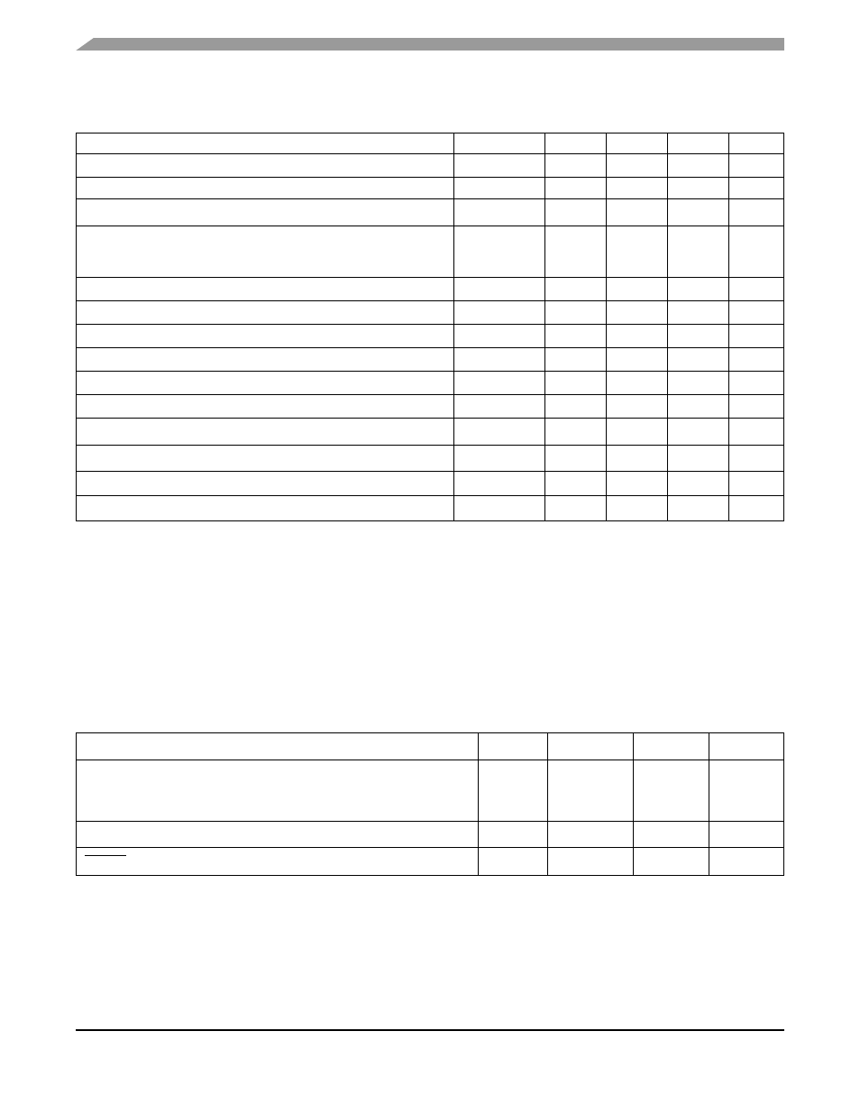
19.6 FLASH Memory Characteristics
19.7 Control Timing
Characteristic
Symbol
Min
Typ
Max
Unit
RAM data retention voltage
V
RDR
1.3
—
—
V
FLASH program bus clock frequency
—
1
—
—
MHz
FLASH read bus clock frequency
f
Read
(1)
1. f
Read
is defined as the frequency range for which the FLASH memory can be read.
0
—
8 M
Hz
FLASH page erase time
<1 K cycles
>1 K cycles
t
Erase
0.9
3.6
1
4
1.1
5.5
ms
FLASH mass erase time
t
MErase
4
—
—
ms
FLASH PGM/ERASE to HVEN setup time
t
NVS
10
—
—
µs
FLASH high-voltage hold time
t
NVH
5
—
—
µs
FLASH high-voltage hold time (mass erase)
t
NVHL
100
—
—
µs
FLASH program hold time
t
PGS
5
—
—
µs
FLASH program time
t
PROG
30
—
40
µs
FLASH return to read time
t
RCV
(2)
2. t
RCV
is defined as the time it needs before the FLASH can be read after turning off the high voltage charge pump, by
clearing HVEN to 0.
1
—
—
µs
FLASH cumulative program HV period
t
HV
(3)
3. t
HV
is defined as the cumulative high voltage programming time to the same row before next erase.
t
HV
must satisfy this condition: t
NVS
+ t
NVH
+ t
PGS
+ (t
PROG
x
32) ≤ t
HV
maximum.
—
—
4
ms
FLASH endurance
(4)
4. Typical endurance was evaluated for this product family. For additional information on how Freescale defines Typical
Endurance, please refer to Engineering Bulletin EB619.
—
10 k
100 k
—
Cycles
FLASH data retention time
(5)
5. Typical data retention values are based on intrinsic capability of the technology measured at high temperature and de-rated
to 25°C using the Arrhenius equation. For additional information on how Freescale defines Typical Data Retention, please
refer to Engineering Bulletin EB618.
—
15
100
—
Years
Characteristic
(1)
1. V
DD
= 5.0 Vdc ± 10%, V
SS
= 0 Vdc; timing shown with respect to 20% V
DD
and 70% V
DD
, unless otherwise noted
Symbol
Min
Max
Unit
Frequency of operation
(2)
Crystal option
External clock option
(3)
2. See
19.8 Serial Peripheral Interface Characteristics
for more information.
3. No more than 10% duty cycle deviation from 50%.
f
OSC
1
dc
(4)
4. Some modules may require a minimum frequency greater than dc for proper operation; see appropriate table for this
information.
8
32.8
MHz
Internal operating frequency
f
OP
—
8.2
MHz
RESET input pulse width low
(5)
5. Minimum pulse width reset is guaranteed to be recognized. It is possible for a smaller pulse width to cause a reset.
t
IRL
50
—
ns