Freescale Semiconductor MC68HC908MR32 User Manual
Page 53
I/O Registers
MC68HC908MR32 • MC68HC908MR16 Data Sheet, Rev. 6.1
Freescale Semiconductor
53
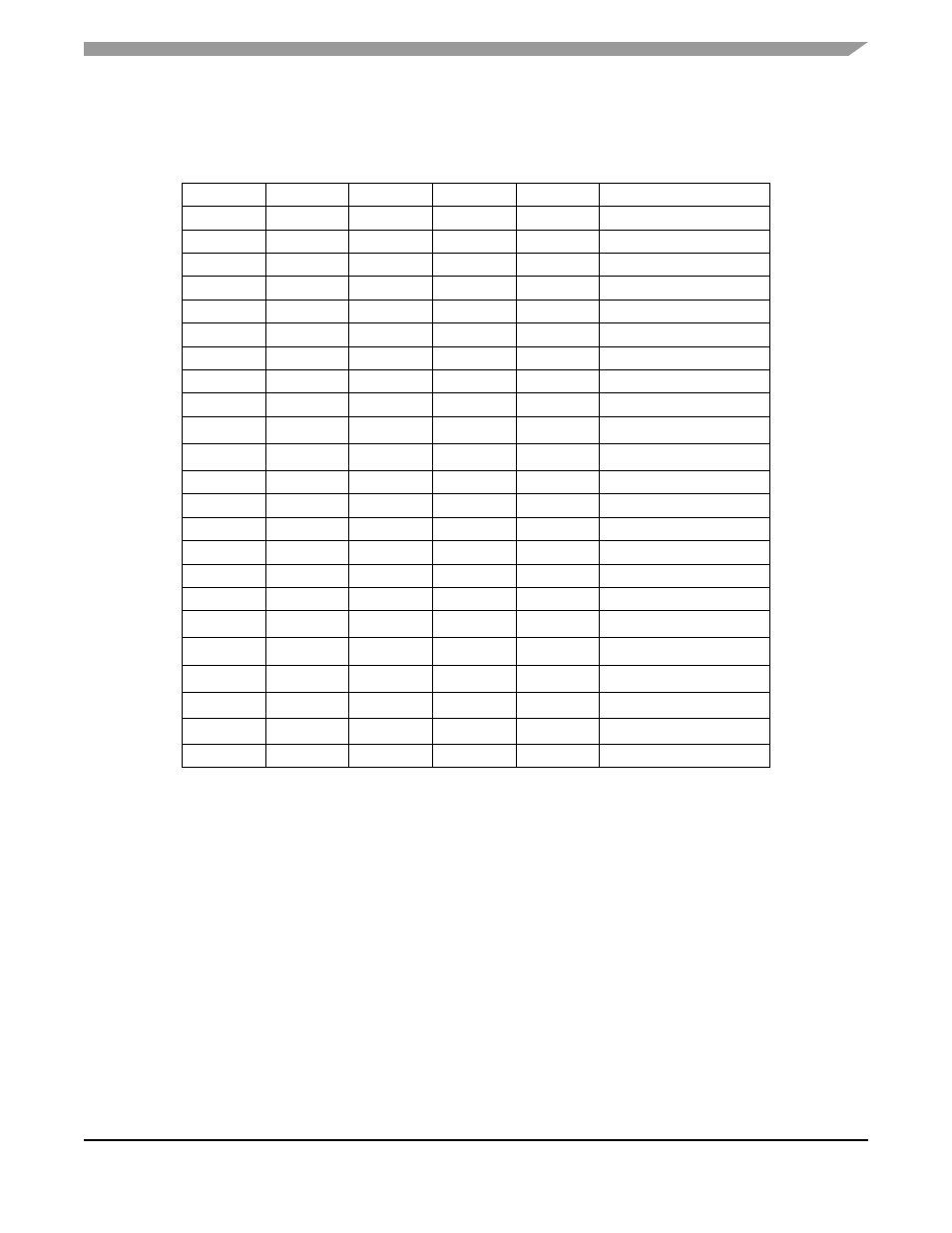
The voltage levels supplied from internal reference nodes as specified in
the operation of the ADC both in production test and for user applications.
Table 3-1. Mux Channel Select
ADCH4
ADCH3
ADCH2
ADCH1
ADCH0
Input Select
0
0
0
0
0
PTB0/ATD0
0
0
0
0
1
PTB1/ATD1
0
0
0
1
0
PTB2/ATD2
0
0
0
1
1
PTB3/ATD3
0
0
1
0
0
PTB4/ATD4
0
0
1
0
1
PTB5/ATD5
0
0
1
1
0
PTB6/ATD6
0
0
1
1
1
PTB7/ATD7
0
1
0
0
0
PTC0/ATD8
0
1
0
0
1
PTC1/ATD9
(1)
1. ATD9 is not available in the 56-pin SDIP package.
0
1
0
1
0
Unused
(2)
0
1
0
1
1
Ш
0
1
1
0
0
Ш
0
1
1
0
1
Ш
0
1
1
1
0
Ш
0
1
1
1
1
Ш
1
0
0
0
0
Ш
1
1
0
1
0
Unused
(2)
2. Used for factory testing.
1
1
0
1
1
Reserved
(3)
3. If any unused channels are selected, the resulting ADC conversion will be unknown.
1
1
1
0
0
Unused
(2)
1
1
1
0
1
V
REFH
1
1
1
1
0
V
REFL
1
1
1
1
1
ADC power off
This manual is related to the following products: