3 pll programming register, Pll programming register, Ppg) — see – Freescale Semiconductor MC68HC908MR32 User Manual
Page 68
Clock Generator Module (CGM)
MC68HC908MR32 • MC68HC908MR16 Data Sheet, Rev. 6.1
68
Freescale Semiconductor
XLD — Crystal Loss Detect Bit
When the VCO output, CGMVCLK, is driving CGMOUT, this read/write bit can indicate whether the
crystal reference frequency is active or not. To check the status of the crystal reference, follow these
steps:
1. Write a logic 1 to XLD.
2. Wait N
× 4 cycles. (N is the VCO frequency multiplier.)
3. Read XLD.
The crystal loss detect function works only when the BCS bit is set, selecting CGMVCLK to drive
CGMOUT. When BCS is clear, XLD always reads as logic 0.
1 = Crystal reference is not active.
0 = Crystal reference is active.
PBWC[3:0] — Reserved for Test
These bits enable test functions not available in user mode. To ensure software portability from
development systems to user applications, software should write 0s to PBWC[3:0] whenever writing to
PBWC.
4.5.3 PLL Programming Register
The PLL programming register (PPG) contains the programming information for the modulo feedback
divider and the programming information for the hardware configuration of the VCO.
MUL[7:4] — Multiplier Select Bits
These read/write bits control the modulo feedback divider that selects the VCO frequency multiplier,
N. See
. A value of $0 in the multiplier select bits
configures the modulo feedback divider the same as a value of $1. Reset initializes these bits to $6 to
give a default multiply value of 6.
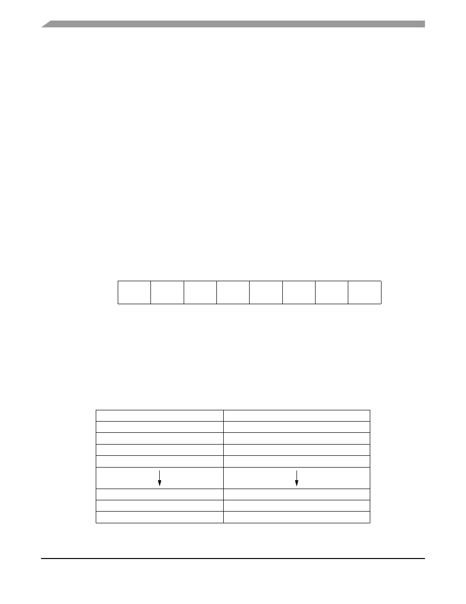
Address: $005E
Bit 7
6
5
4
3
2
1
Bit 0
Read:
MUL7
MUL6
MUL5
MUL4
VRS7
VRS6
VRS5
VRS4
Write:
Reset:
0
1
1
0
0
1
1
0
Figure 4-7. PLL Programming Register (PPG)
Table 4-2. VCO Frequency Multiplier (N) Selection
MUL7:MUL6:MUL5:MUL4
VCO Frequency Multiplier (N)
0000
1
0001
1
0010
2
0011
3
1101
13
1110
14
1111
15