1 polled lvi operation, 2 forced reset operation, 3 false reset protection – Freescale Semiconductor MC68HC908MR32 User Manual
Page 98: 4 lvi trip selection, Polled lvi operation, Forced reset operation, False reset protection, Lvi trip selection, Figure 9-2
Low-Voltage Inhibit (LVI)
MC68HC908MR32 • MC68HC908MR16 Data Sheet, Rev. 6.1
98
Freescale Semiconductor
Once an LVI reset occurs, the MCU remains in reset until V
DD
rises above a voltage, V
LVRX
+ V
LVHX
.
V
DD
must be above V
LVRX
+ V
LVHX
for only one CPU cycle to bring the MCU out of reset. See
14.3.2.6 Low-Voltage Inhibit (LVI) Reset
. The output of the comparator controls the state of the LVIOUT
flag in the LVI status register (LVISCR).
An LVI reset also drives the RST pin low to provide low-voltage protection to external peripheral devices.
See
19.5 DC Electrical Characteristics
9.3.1 Polled LVI Operation
In applications that can operate at V
DD
levels below V
LVRX
, software can monitor V
DD
by polling the
LVIOUT bit. In the configuration register, the LVIPWR bit must be 1 to enable the LVI module, and the
LVIRST bit must be 0 to disable LVI resets. See
Chapter 5 Configuration Register (CONFIG)
in the LVISCR selects V
LVRX
.
9.3.2 Forced Reset Operation
In applications that require V
DD
to remain above V
LVRX
, enabling LVI resets allows the LVI module to
reset the MCU when V
DD
falls to the V
LVRX
level and remains at or below that level for nine or more
consecutive CPU cycles. In the CONFIG register, the LVIPWR and LVIRST bits must be 1s to enable the
LVI module and to enable LVI resets. TRPSEL in the LVISCR selects V
LVRX
.
9.3.3 False Reset Protection
The V
DD
pin level is digitally filtered to reduce false resets due to power supply noise. In order for the LVI
module to reset the MCU, V
DD
must remain at or below V
LVRX
for nine or more consecutive CPU cycles.
V
DD
must be above V
LVRX
+ V
LVHX
for only one CPU cycle to bring the MCU out of reset. TRPSEL in the
LVISCR selects V
LVRX
+ V
LVHX
.
9.3.4 LVI Trip Selection
The TRPSEL bit allows the user to chose between 5 percent and 10 percent tolerance when monitoring
the supply voltage. The 10 percent option is enabled out of reset. Writing a 1 to TRPSEL will enable 5
percent option.
NOTE
The microcontroller is guaranteed to operate at a minimum supply voltage.
The trip point (VLVR1 or VLVR2) may be lower than this. See
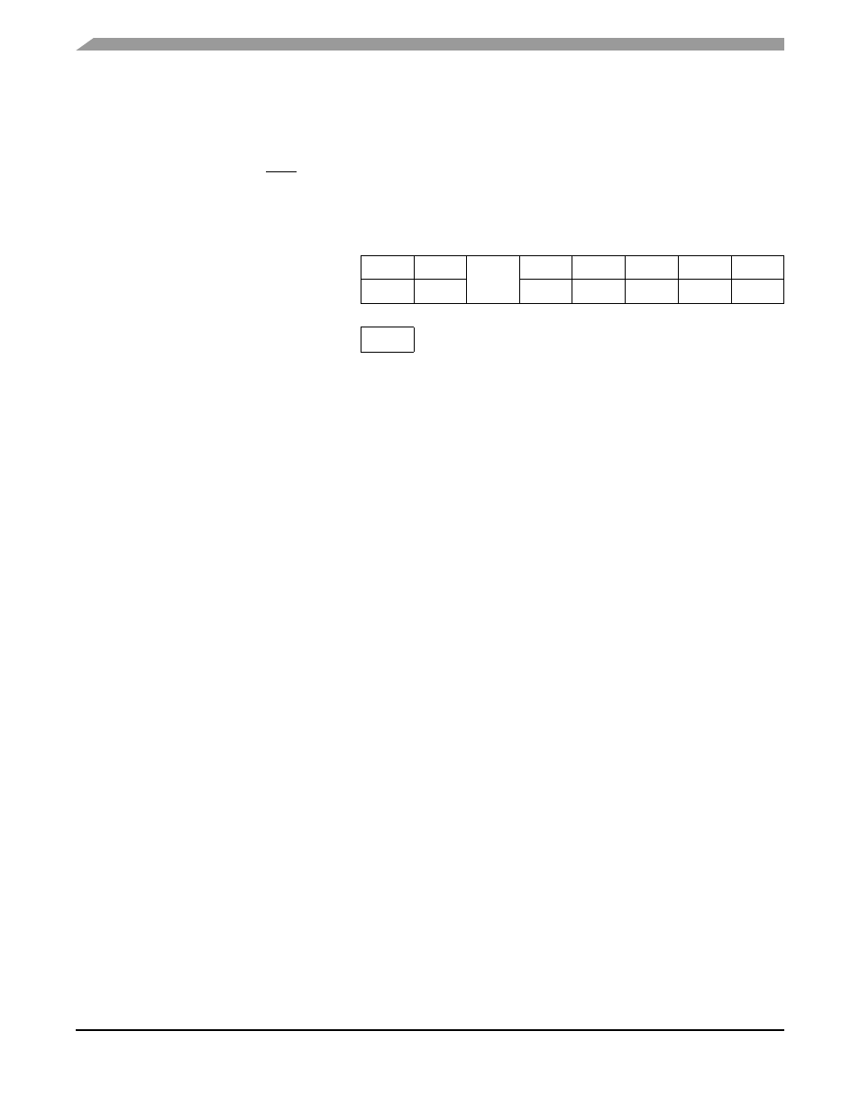
Addr.
Register Name
Bit 7
6
5
4
3
2
1
Bit 0
$FE0F
LVI Status and Control Register
(LVISCR)
Read: LVIOUT
0
TRPSEL
0
0
0
0
0
Write:
R
R
R
R
R
R
R
Reset:
0
0
0
0
0
0
0
0
R
= Reserved
Figure 9-2. LVI I/O Register Summary