Freescale Semiconductor MC68HC908MR32 User Manual
Page 34
Memory
MC68HC908MR32 • MC68HC908MR16 Data Sheet, Rev. 6.1
34
Freescale Semiconductor
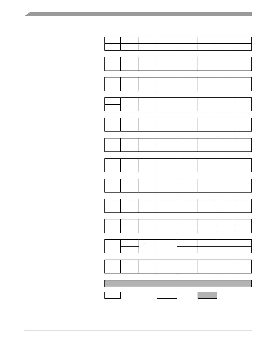
$0053
TIMB Counter Register Low
(TBCNTL)
Read:
Bit 7
Bit 6
Bit 5
Bit 4
Bit 3
Bit 2
Bit 1
Bit 0
Write:
R
R
R
R
R
R
R
R
Reset:
0
0
0
0
0
0
0
0
$0054
TIMB Counter Modulo Register
High (TBMODH)
Read:
Bit 15
Bit 14
Bit 13
Bit 12
Bit 11
Bit 10
Bit 9
Bit 8
Write:
Reset:
1
1
1
1
1
1
1
1
$0055
TIMB Counter Modulo Register
Low (TBMODL)
Read:
Bit 7
Bit 6
Bit 5
Bit 4
Bit 3
Bit 2
Bit 1
Bit 0
Write:
Reset:
1
1
1
1
1
1
1
1
$0056
TIMB Channel 0 Status/Control
Register (TBSC0)
Read:
CH0F
CH0IE
MS0B
MS0A
ELS0B
ELS0A
TOV0
CH0MAX
Write:
0
Reset:
0
0
0
0
0
0
0
0
$0057
TIMB Channel 0 Register High
(TBCH0H)
Read:
Bit 15
Bit 14
Bit 13
Bit 12
Bit 11
Bit 10
Bit 9
Bit 8
Write:
Reset:
Indeterminate after reset
$0058
TIMB Channel 0 Register Low
(TBCH0L)
Read:
Bit 7
Bit 6
Bit 5
Bit 4
Bit 3
Bit 2
Bit 1
Bit 0
Write:
Reset:
Indeterminate after reset
$0059
TIMB Channel 1 Status/Control
Register (TBSC1)
Read:
CH1F
CH1IE
0
MS1A
ELS1B
ELS1A
TOV1
CH1MAX
Write:
0
R
Reset:
0
0
0
0
0
0
0
0
$005A
TIMB Channel 1 Register High
(TBCH1H)
Read:
Bit 15
Bit 14
Bit 13
Bit 12
Bit 11
Bit 10
Bit 9
Bit 8
Write:
Reset:
Indeterminate after reset
$005B
TIMB Channel 1 Register Low
(TBCH1L)
Read:
Bit 7
Bit 6
Bit 5
Bit 4
Bit 3
Bit 2
Bit 1
Bit 0
Write:
Reset:
Indeterminate after reset
$005C
PLL Control Register
(PCTL)
Read:
PLLIE
PLLF
PLLON
BCS
1
1
1
1
Write:
R
R
R
R
R
Reset:
0
0
1
0
1
1
1
1
$005D
PLL Bandwidth Control
Register (PBWC)
Read:
AUTO
LOCK
ACQ
XLD
0
0
0
0
Write:
R
R
R
R
R
Reset:
0
0
0
0
0
0
0
0
$005E
PLL Programming Register
(PPG)
Read:
MUL7
MUL6
MUL5
MUL4
VRS7
VRS6
VRS5
VRS4
Write:
Reset:
0
1
1
0
0
1
1
0
$005F
Unimplemented
Addr.
Register Name
Bit 7
6
5
4
3
2
1
Bit 0
U = Unaffected
X = Indeterminate
R
= Reserved
Bold
= Buffered
= Unimplemented
Figure 2-2. Control, Status, and Data Registers Summary (Sheet 7 of 8)